Semiconductor array

Active Publication Date: 2009-04-02
NXP USA INC +1
View PDF10 Cites 142 Cited by
  • Summary
  • Abstract
  • Description
  • Claims
  • Application Information

AI Technical Summary

Benefits of technology

[0021]If there is a selection line that is not coupled to both cells, it may be possible to read/write data from/into a number of cells without disturbing the cells of ot

Problems solved by technology

Furthermore, the dimensions of the semiconductor array tend to shrink, i.e., the section of the control line crossed by the

Method used


Image

  • Semiconductor array
  • Semiconductor array
  • Semiconductor array

Examples


Embodiment Construction

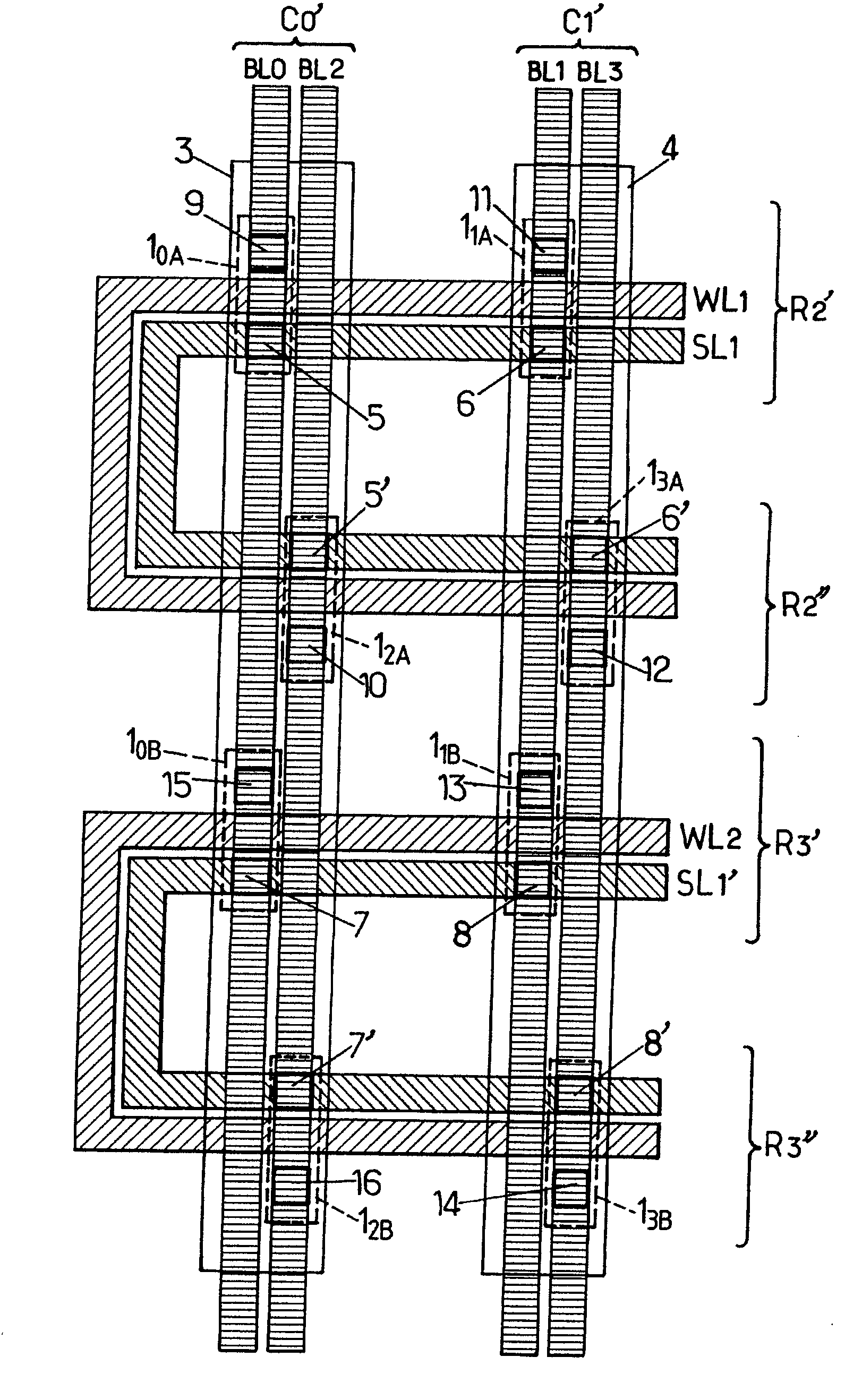
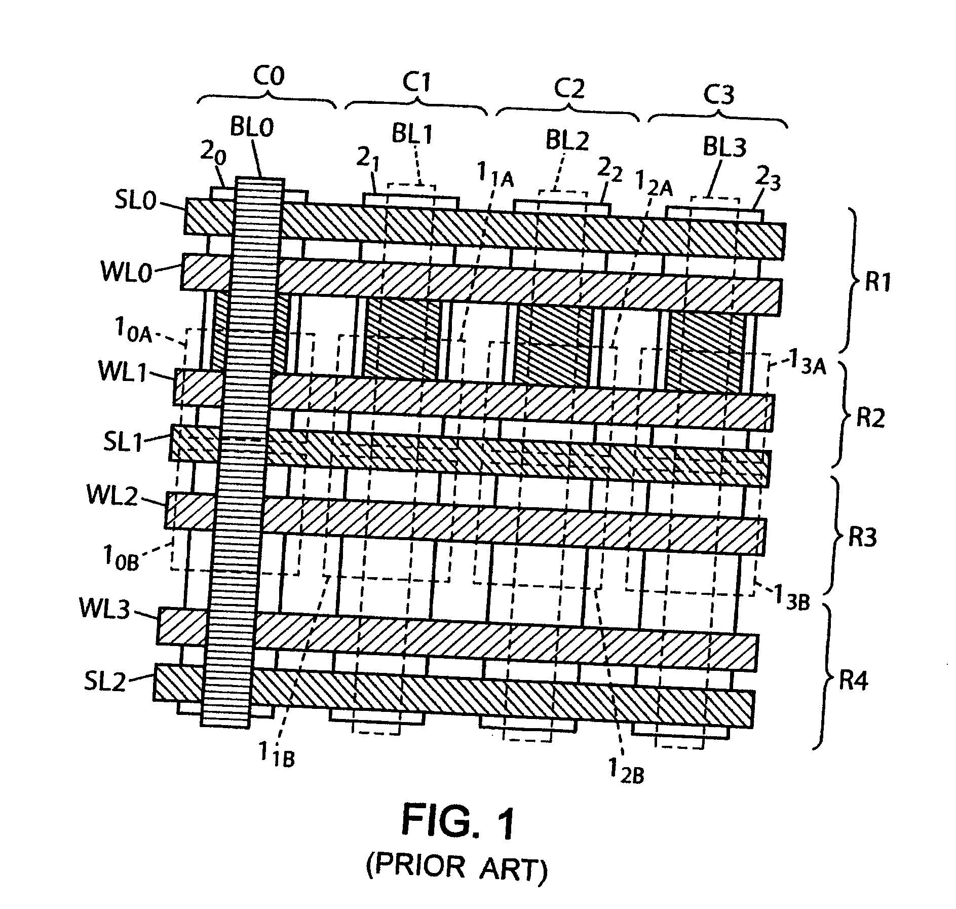
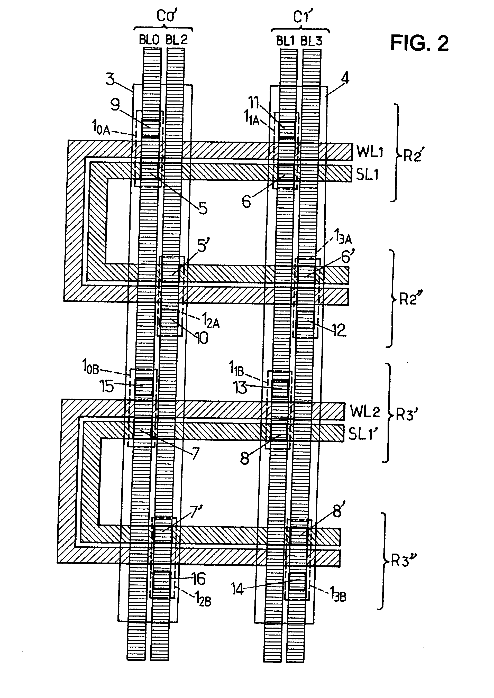
[0028]In the following description, numerous specific details are given to provide a thorough understanding of embodiments. The embodiments can be practiced without one or more of the specific details, or with other methods, components, materials, etc. In other instances, well-known structures, materials, or operations are not shown or described in detail to avoid obscuring aspects of the embodiments.

[0029]Reference throughout this specification to “one embodiment” or “an embodiment” means that a particular feature, structure, or characteristic described in connection with the embodiment is included in at least one embodiment. Thus, the appearances of the phrases “in one embodiment” or “in an embodiment” in various places throughout this specification are not necessarily all referring to the same embodiment. Furthermore, the particular features, structures, or characteristics may be combined in any suitable manner in one or more embodiments.

[0030]The headings provided herein are for...


PUM


Abstract

A semiconductor array includes a matrix of cells, the matrix being arranged in rows and columns of cells, and a plurality of control lines. Each cell is coupled to a number of control lines allowing to select and read/write said cell. At least one of said control lines is coupled to cells of a plurality of columns and of at least two rows of the matrix.

Description

TECHNICAL FIELD[0001]The present disclosure generally relates to semiconductor arrays.[0002]Although the present description focuses mainly on floating body memory arrays, the possible fields of application of the embodiments are manifold. For example, embodiments may also include CMOS memory arrays, or even programmable logic arrays such as PLAs.BACKGROUND INFORMATION[0003]A memory array comprises a plurality of memory cells, or cells, and is organized into rows and columns of such cells. A column extends over the matrix in a vertical direction, whereas a row extends over the matrix in a horizontal direction. The cell that lies at the ith row and the jth column is called the i,j cell. The cells of a same column have a same j index, the i index varying from 1 to the number of rows of the matrix. The cells of a same row have a same i index, the j index varying from 1 to the number of columns of the matrix.[0004]Each cell may comprise one or more storing elements, e.g., transistor(s) ...

Claims


Application Information

Patent Timeline
IPC IPC(8): G11C11/34
CPCG11C11/4023H01L27/1052G11C11/405G11C2211/4016H01L21/8232H01L21/84H01L27/0207H01L27/10H01L27/105H01L27/108H01L27/10802H01L27/10882H01L27/115H01L27/11521H01L27/118H01L27/11803H01L27/12H01L27/1203H01L29/7841G11C11/4026H10B12/20H10B99/00H10B12/00H10B12/48H10B69/00H10B41/30
Inventor FERRANT, RICHARDGENEVAUX, FRANCKBURNETT, DAVIDGOUYA, GERALDMALINGE, PIERRE
Owner NXP USA INC
Why Eureka
Try Eureka