
Film position adjusting method, memory medium and substrate processing system

a technology of memory media and substrate, applied in the direction of chemical vapor deposition coating, semiconductor/solid-state device testing/measurement, coating, etc., can solve the problem of small measurement error

Active Publication Date: 2009-04-02
TOKYO ELECTRON LTD
View PDF5 Cites 5 Cited by
  • Summary
  • Abstract
  • Description
  • Claims
  • Application Information

AI Technical Summary

Benefits of technology

[0007]In view of the above, the present invention provides a technique capable of correcting a discrepancy between a position of a formed film and a reference position of a film.
[0010]In accordance with the present invention, it is unnecessary to unload the substrate from the substrate processing system and, also, the operator does not need to input the calculated position discrepancy to the substrate processing system. Moreover, since the width of the non-film forming portion is measured not by the operator but by the image sensor, the measurement error is small. Accordingly, the discrepancy between a formed film position and a reference position of a film can be easily corrected.
[0012]Since the width of the non-film forming portion is measured on a peripheral portion of the substrate at locations which are 90° apart in a circumference direction, it is possible to easily calculate the central position of the formed film so that the discrepancy between a formed film position and a reference position of a film can be easily calculated.
[0018]Accordingly, it is possible to prevent the non-film forming portion from being deviated from the range where an image can be recognized by the image sensor and, thus, the width of the non-film forming portion can be effectively measured.

Problems solved by technology

Moreover, since the width of the non-film forming portion is measured not by the operator but by the image sensor, the measurement error is small.

Method used


Image

  • Film position adjusting method, memory medium and substrate processing system
  • Film position adjusting method, memory medium and substrate processing system
  • Film position adjusting method, memory medium and substrate processing system

Examples


Embodiment Construction

[0029]The embodiments of the present invention will be described with reference to the accompanying drawings which form a part hereof.

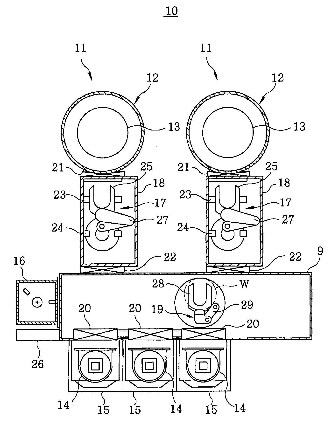
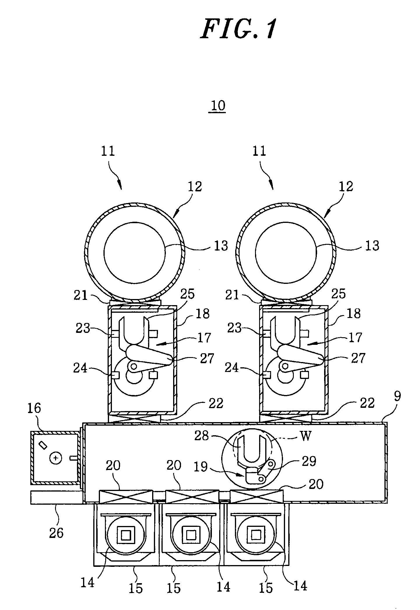
[0030]First of all, a substrate processing system in accordance with an embodiment of the present invention will be described. FIG. 1 is a top view schematically showing a configuration of a substrate processing system in accordance with an embodiment of the present invention.

[0031]As shown in FIG. 1, the substrate processing system 10 includes a plurality of process ships 11 for performing a film forming process using a plasma, such as CVD treatment, on to a circular plate-shaped wafer W, and a loader module 9 as a common transfer chamber having a square cross section, the process ships 11 being connected to the loader module 9.

[0032]Further, the loader module 9 has connected thereto three FOUP mounting tables 15 on each of which is mounted a FOUP (front opening unified pod) 14 as a container for housing twenty-five wafers W, and an orienter (centeri...


PUM

PropertyMeasurementUnit
Angleaaaaaaaaaa
Widthaaaaaaaaaa

Abstract

A substrate processing system includes a processing chamber 12, and an orienter 16 centering a wafer W. The orienter 16 is provided with an orienter sensor 42 measuring a central position discrepancy of the wafer W, and an image sensor 41 measuring a width of a non-film forming portion at circumferential portions of the wafer W. After a film deposition processing in the processing chamber 12, the wafer W is loaded into the orienter 16 where a central position discrepancy of the wafer W is measured, and the wafer W is then centered. Further, the width of the non-film forming portion of the wafer W is measured, and a film position discrepancy is calculated based on the width of the non-film forming portion. To correct the calculated film position discrepancy, a target transfer position of the wafer W on a mounting table 13 in the processing chamber 12 is adjusted.

Description

FIELD OF THE INVENTION[0001]The present invention relates to a film position adjusting method, a storage medium and a substrate processing system; and, more particularly, to a film position adjusting method for correcting a discrepancy of a position of a film formed on a surface of a substrate.BACKGROUND OF THE INVENTION[0002]There is a substrate processing system having a processing chamber for forming an insulating film or a metal film for forming wiring or the like by CVD (Chemical Vapor Deposits) on a surface of a circular plate-shaped wafer as a substrate. In this substrate processing system, when a film is formed in a substantially circular shape on the wafer surface, it is preferable that the center of the wafer coincides with that of the film. However, a discrepancy of an actual film forming position (an actual film position where a film is formed by treatment) with respect to a reference film forming position (a target film position where a film should be formed) (hereinaft...

Claims


Application Information

Patent Timeline
IPC IPC(8): C23C16/52
CPCC23C16/04C23C16/52H01L21/681H01L21/67288H01L21/67259
Inventor SASAKI, YOSHIAKIYAMAGUCHI, HIROFUMI
Owner TOKYO ELECTRON LTD
Learn More