Semiconductor Device Package

a technology of semiconductor devices and connectors, applied in the direction of optics, instruments, optical elements, etc., can solve the problems of increasing the number of operations required to manufacture the difficulty of applying the above-described connector structure to the semiconductor device package, so as to reduce manufacturing operations and manufacturing efficient

Inactive Publication Date: 2009-04-09
KK TOKAI RIKA DENKI SEISAKUSHO
View PDF6 Cites 2 Cited by
  • Summary
  • Abstract
  • Description
  • Claims
  • Application Information

AI Technical Summary

Benefits of technology

[0012]The present invention provides a semiconductor device package incorporating a connector that reduces manufacturing operations and enables efficient manufacturing.

Problems solved by technology

However, the connector structure described in Japanese Laid-Open Patent Publication No. 2003-115630 is limited to a structure in which a coaxial connector and coaxial cable are electrically connected to and disconnected from each other.
For example, it would be difficult to apply the above-described connector structure to a semiconductor device package in which plural sets of terminals, such as those of a magnetic detector, are connected and disconnected.
This increases the number of operations required to manufacture the semiconductor device package that incorporates a connector.

Method used


Image

  • Semiconductor Device Package
  • Semiconductor Device Package
  • Semiconductor Device Package

Examples


first embodiment

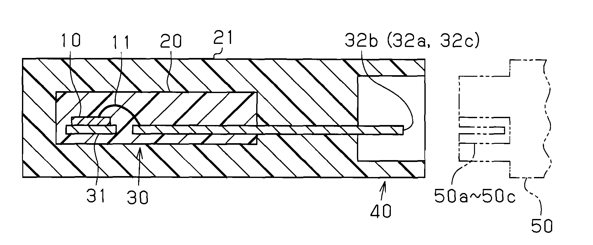
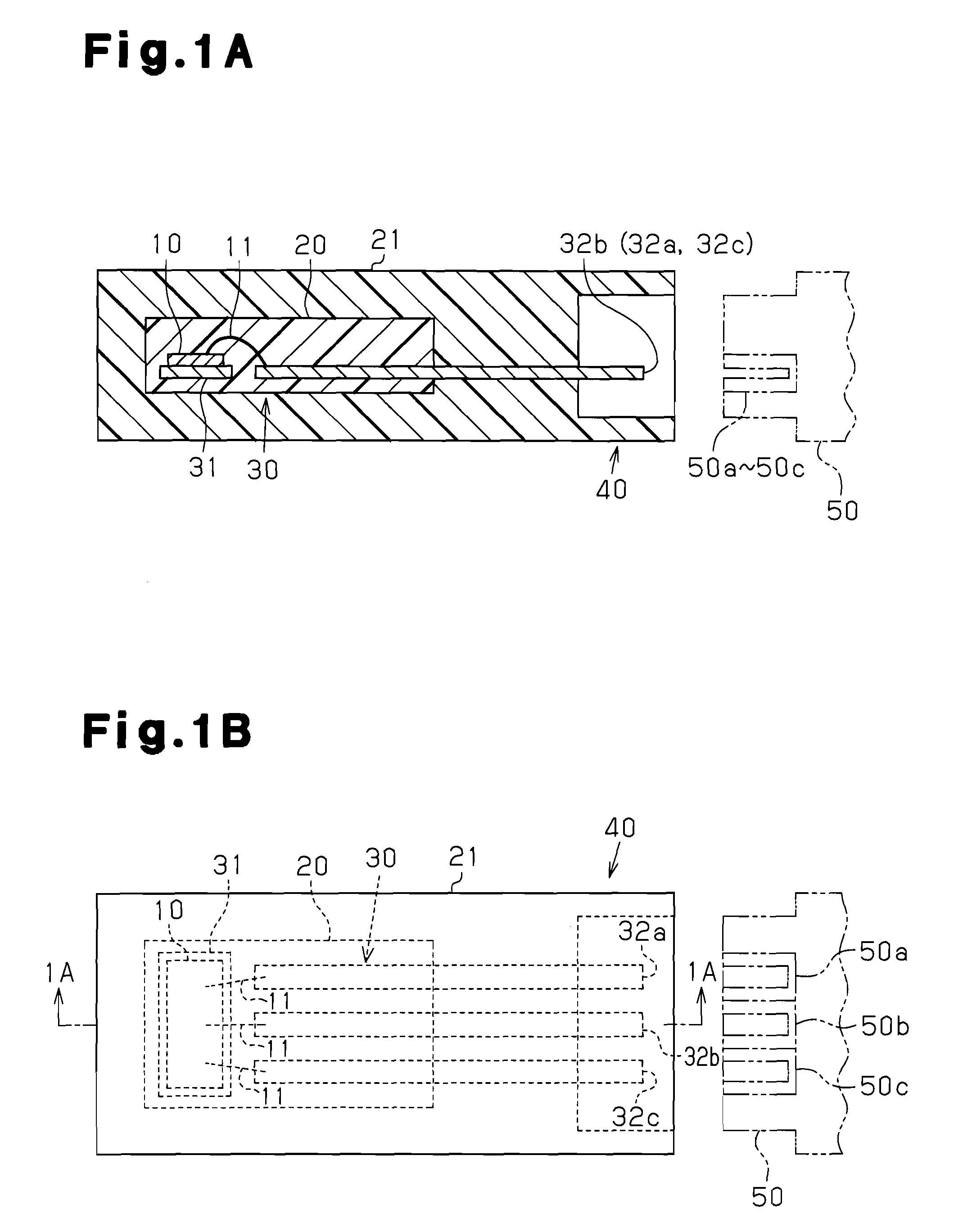
[0026]a semiconductor device package that incorporates a connector according to the present invention will now be discussed with reference to FIGS. 1 to 3.

[0027]As shown in FIGS. 1A and 1B, in the first embodiment, the semiconductor device package covers a semiconductor device 10 with resin members 20 and 21 to protect the semiconductor device 10 from the ambient environment in a manner similar to the semiconductor device package shown in FIGS. 7A and 7B. The resin member 21 includes a connector guide 40, which forms part of the connector. The connector guide 40 is used to guide insertion of a holder 50, which holds socket terminals 50a to 50c (shown by broken lines in FIGS. 1A and 1B).

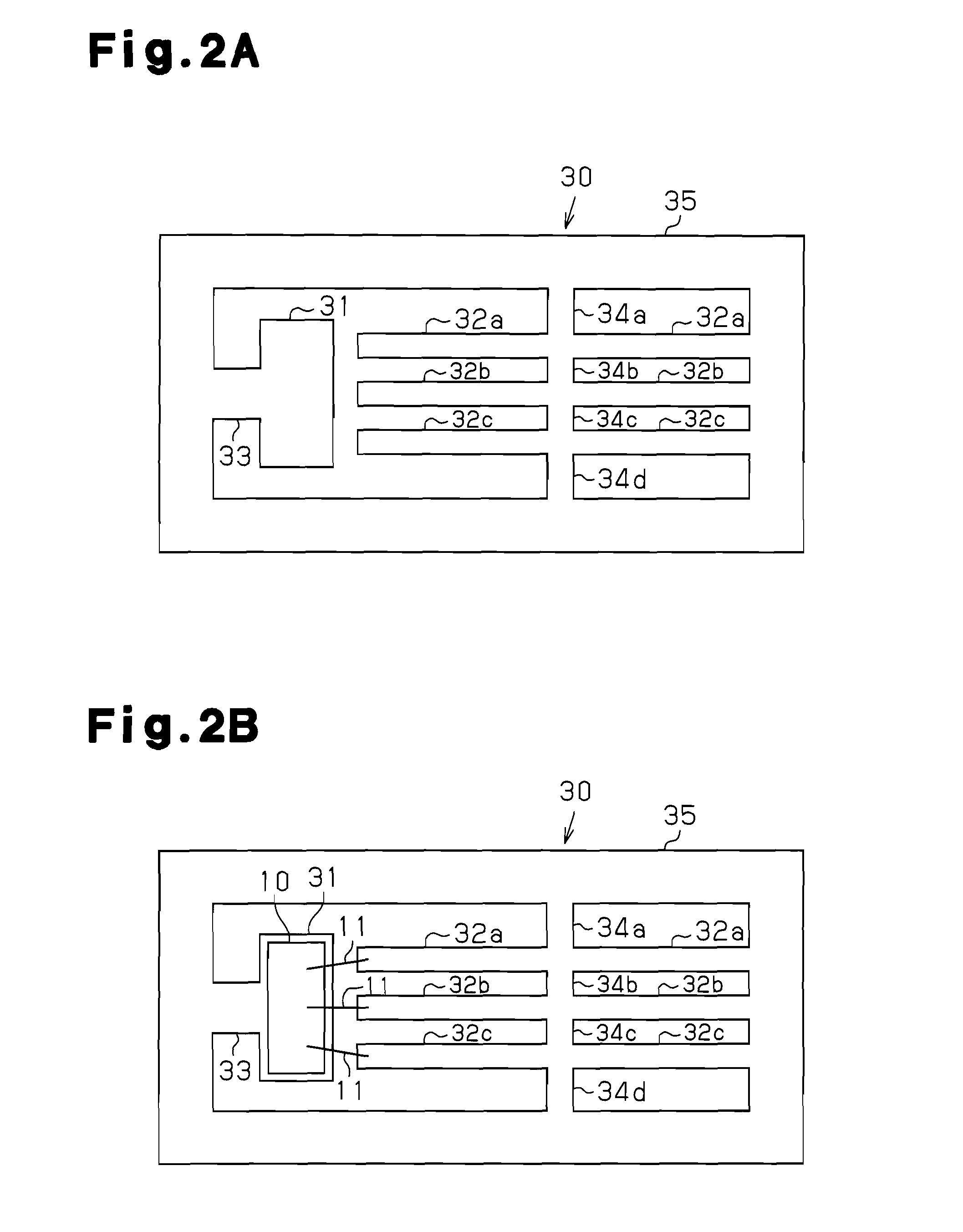
[0028]The semiconductor device 10 is fixed to a chip support 31 of a lead frame 30. The lead frame 30 includes leads 32a to 32c, which are electrically connected to the semiconductor device 10 by bonding wires 11. The resin member 20 is molded so as to envelop the semiconductor device 10, the bonding ...

second embodiment

[0044]The second embodiment adds a new operation in which the leads 72a to 72c are folded when manufacturing the semiconductor device package that incorporates a connector. However, the two operations of adhering and bonding as in the prior art process for manufacturing a semiconductor device package do not have to be performed. This reduces the total number of manufacturing operations.

[0045]In the second embodiment, the semiconductor device package has the advantages described below.

[0046](3) The long leads 72a to 72c are folded to form the plug terminals. Thus, even though the leads 72a to 72c do not have the thickness and rigidity required for use as plug terminals, the folded overlapping portions of the leads 72a to 72c ensures the thickness and rigidity required for plug terminals. This maintains reliability as a connector in an optimal manner.

[0047](4) The long leads 72a to 72c are folded to form the plug terminals when the primary molded product is formed. Further, the connec...


PUM


Abstract

A semiconductor device package incorporating a connector that reduces manufacturing operations and enables efficient manufacturing. The semiconductor device package includes a primary molded product and a secondary molded product. The primary molded product includes a semiconductor device, a lead connected to the semiconductor device, and a plug terminal formed by at least part of the lead. The primary molded product envelops the semiconductor device and part of the lead in a first resin material. The secondary molded product envelops the primary molded product in a second resin material and includes a connector guide surrounding the plug terminal and used to guide insertion of a holder holding a socket terminal connectable to the plug terminal.

Description

BACKGROUND OF THE INVENTION[0001]The present invention relates to a semiconductor device package incorporating a connector.[0002]In the prior art, a so-called semiconductor device package covers a semiconductor device with resin to protect the semiconductor device from the ambient environment. One type of such a semiconductor device package incorporates a connector. The connector includes a plug terminal and a connector guide. The plug terminal is electrically connected to the semiconductor device by a lead or the like. The connector guide is used to guide the insertion of a holder that holds a socket terminal. Insertion of the holder into the connector guide connects the socket terminal and plug terminal. Japanese Laid-Open Patent Publication No. 2003-115630 describes such a semiconductor device package that incorporates a connector. FIG. 6 is a cross-sectional view showing the semiconductor device package described in Japanese Laid-Open Patent Publication No. 2003-115630.[0003]As ...

Claims


Application Information

Patent Timeline
Patent Type & Authority Applications(United States)
IPC IPC(8): H01L21/60H01L23/498
CPCG02B6/4201H01L21/565H01L23/49555H01L2224/48091H01L24/48H01L2924/01079H01L23/3107H01L2224/49171H01L2224/48247H01L2924/00014H01L2924/00H01L2924/181H01L24/49H01L2924/00012H01L2224/45099H01L2224/45015H01L2924/207
Inventor TAJIMA, MASAYA
Owner KK TOKAI RIKA DENKI SEISAKUSHO
Why Eureka
Try Eureka