Printed circuit board and method for manufacturing the same

a technology of printed circuit board and printed circuit, which is applied in the direction of printed circuit aspects, resist details, conductive pattern formation, etc., can solve the problems of signal noise, limit the density of circuit board, and the thickness of the plating layer formed using the plating bar may not be uniform,

Inactive Publication Date: 2009-04-16
SAMSUNG ELECTRO MECHANICS CO LTD
View PDF9 Cites 16 Cited by
  • Summary
  • Abstract
  • Description
  • Claims
  • Application Information

AI Technical Summary

Problems solved by technology

These plating bars, however, may impose a limit on the density of circuits, entail an extra process of removing the plating bars, and cause signal noise when there is residue left from the plating bars.
In addition, the plating layer formed using the plating bars may not have a uniform thickness, and may be formed beyond the areas of the circuit pattern in which the pads are intended to be formed.

Method used


Image

  • Printed circuit board and method for manufacturing the same
  • Printed circuit board and method for manufacturing the same
  • Printed circuit board and method for manufacturing the same

Examples


Embodiment Construction

[0026]Certain embodiments of the invention will be described below in more detail with reference to the accompanying drawings. Those components that are the same or are in correspondence are rendered the same reference numeral regardless of the figure number, and redundant explanations are omitted.

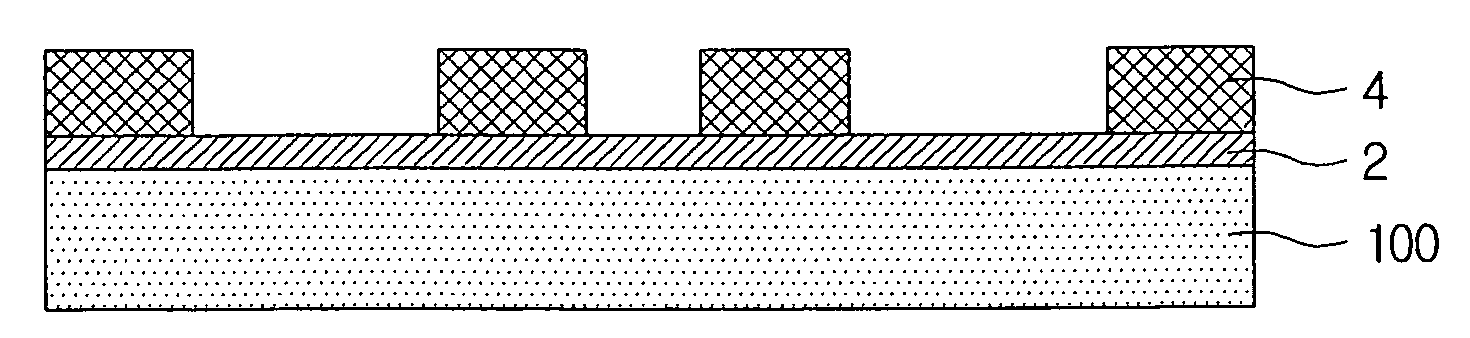
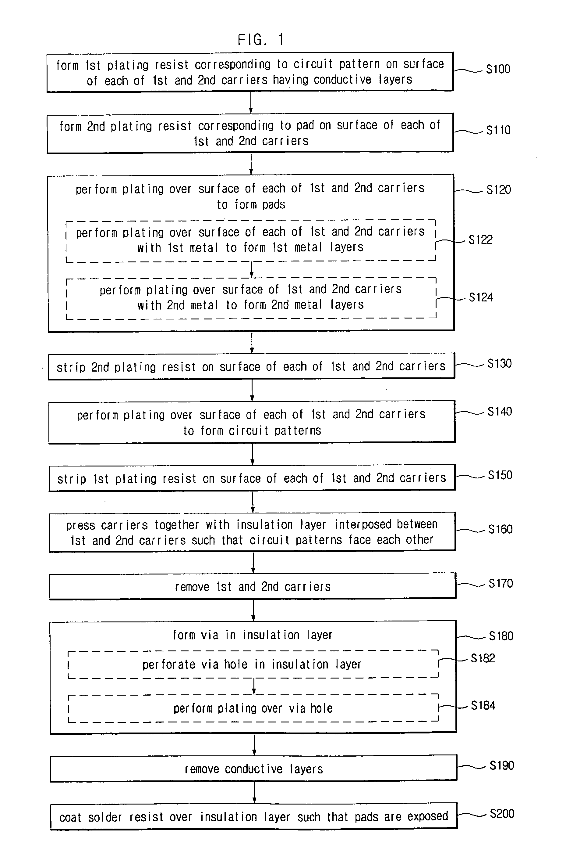
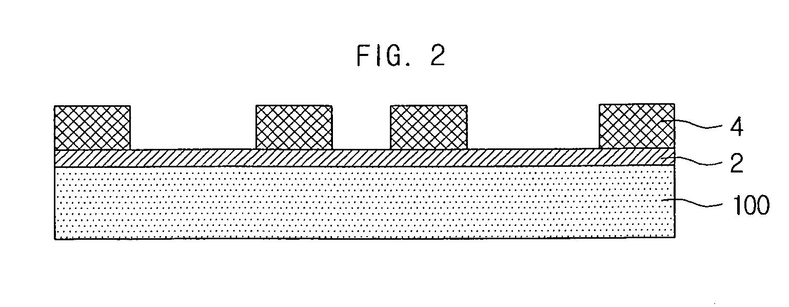
[0027]FIG. 1 is a flowchart illustrating a method of manufacturing a printed circuit board according to an embodiment of the invention, FIG. 2 through FIG. 8 are cross-sectional views representing a method of forming a circuit pattern and a pad on a first carrier, according to an embodiment of the invention, and FIG. 9 through FIG. 15 are cross-sectional views representing a method of forming a circuit pattern and pads on a second carrier, according to an embodiment of the invention. Also, FIG. 16 through FIG. 22 are cross-sectional views representing a method of manufacturing a printed circuit board according to an embodiment of the invention. In FIGS. 2 to 20 are illustrated a first carr...


PUM

PropertyMeasurementUnit
thicknessaaaaaaaaaa
thicknessaaaaaaaaaa
photosensitiveaaaaaaaaaa

Abstract

A printed circuit board and a method for manufacturing the same are disclosed. The manufacturing method includes: forming a first plating resist corresponding to the circuit pattern on a surface of each of a first carrier and a second carrier; forming a second plating resist corresponding to the pad on each of the surfaces; forming the pad by performing plating over each of the surfaces; stripping the second plating resists; forming the circuit pattern by performing plating over each of the surfaces; pressing the first carrier and the second carrier with an insulation layer interposed between the first carrier and the second carrier such that the circuit patterns face each other; and removing the first carrier and the second carrier. Since plating bars need not be used, the degree of freedom in designing circuits can be increased, and circuits of higher densities can be designed.

Description

CROSS-REFERENCE TO RELATED APPLICATIONS[0001]This application claims the benefit of Korean Patent Application No. 10-2007-0103894 filed with the Korean Intellectual Property Office on Oct. 16, 2007, the disclosure of which is incorporated herein by reference in its entirety.BACKGROUND[0002]1. Technical Field[0003]The present invention relates to a printed circuit board and a method for manufacturing the printed circuit board.[0004]2. Description of the Related Art[0005]In spite of the recent trends towards lighter, thinner, and smaller integrated circuit chips, the number of leads in an IC package is increasing. To counter this, it has become common to use package boards such as of BGA (ball grid array) and CSP (chip scale package) types.[0006]As it is easy to increase the density of the board by using solder balls, many boards are used as package boards on which semiconductor chips can be mounted. A gold plating process may be performed to improve the electrical connection of the w...

Claims


Application Information

Patent Timeline
Patent Type & Authority Applications(United States)
IPC IPC(8): H05K1/00H05K3/02
CPCH01L21/4846H05K3/205H05K3/243Y10T29/49155H05K2201/09481H05K2203/0376H05K2203/0574H05K3/421H05K3/18
Inventor PARK, JUNG-HYUNKIM, JI-EUNKANG, MYUNG-SAM
Owner SAMSUNG ELECTRO MECHANICS CO LTD
Why Eureka
Try Eureka