
Light emitting device

Inactive Publication Date: 2009-04-16
PANASONIC CORP
View PDF19 Cites 40 Cited by
  • Summary
  • Abstract
  • Description
  • Claims
  • Application Information

AI Technical Summary

Benefits of technology

[0009]In view of the above problem, the present invention has been accomplished and has an object of providing a light emitting device and a method of manufacturing the same capable of improving a light output as well as its reliability.

Problems solved by technology

In addition, when used as a material of the encapsulation member, the epoxy resin exhibits only lower weatherability than the silicone one.
However, since a linear expansion coefficient of the silicone resin, which is a material of the encapsulation member, is more than 10 times that of an aluminum which is a material of the frame, voids may be generated within the encapsulation member due to a difference in linear expansion coefficient between silicone resin and aluminum.
Furthermore, in the light emitting device, although the light emitted from the LED chip can be taken to external of the encapsulation member effectively by means of the frame with a mirror interior face, there is a failure of causing light loss resulting from the reflection of the light on the interior face of the frame.
Besides, in the light emitting device according to the Patent document 1, when a lens controlling an orientation of the light emitted from the LED chip is arranged over the encapsulation member and the frame, a light output may be lowered due to a deviation in an optical axis between the LED chip and the lens, resulting from dimensional inaccuracy of the flame and the lens or positioning inaccuracy thereof.
However, the encapsulation member is likely to suffer from an external force to develop a stress transmittable to the LED chip and the bonding wires.

Method used


Image

  • Light emitting device
  • Light emitting device
  • Light emitting device

Examples


first embodiment

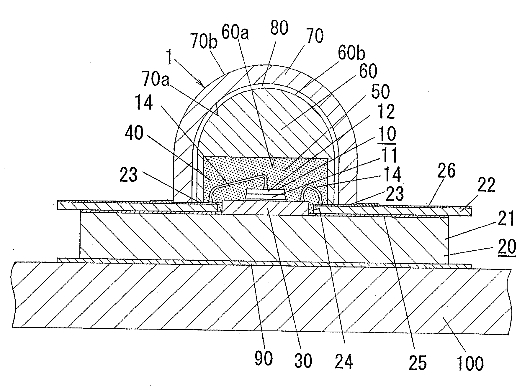
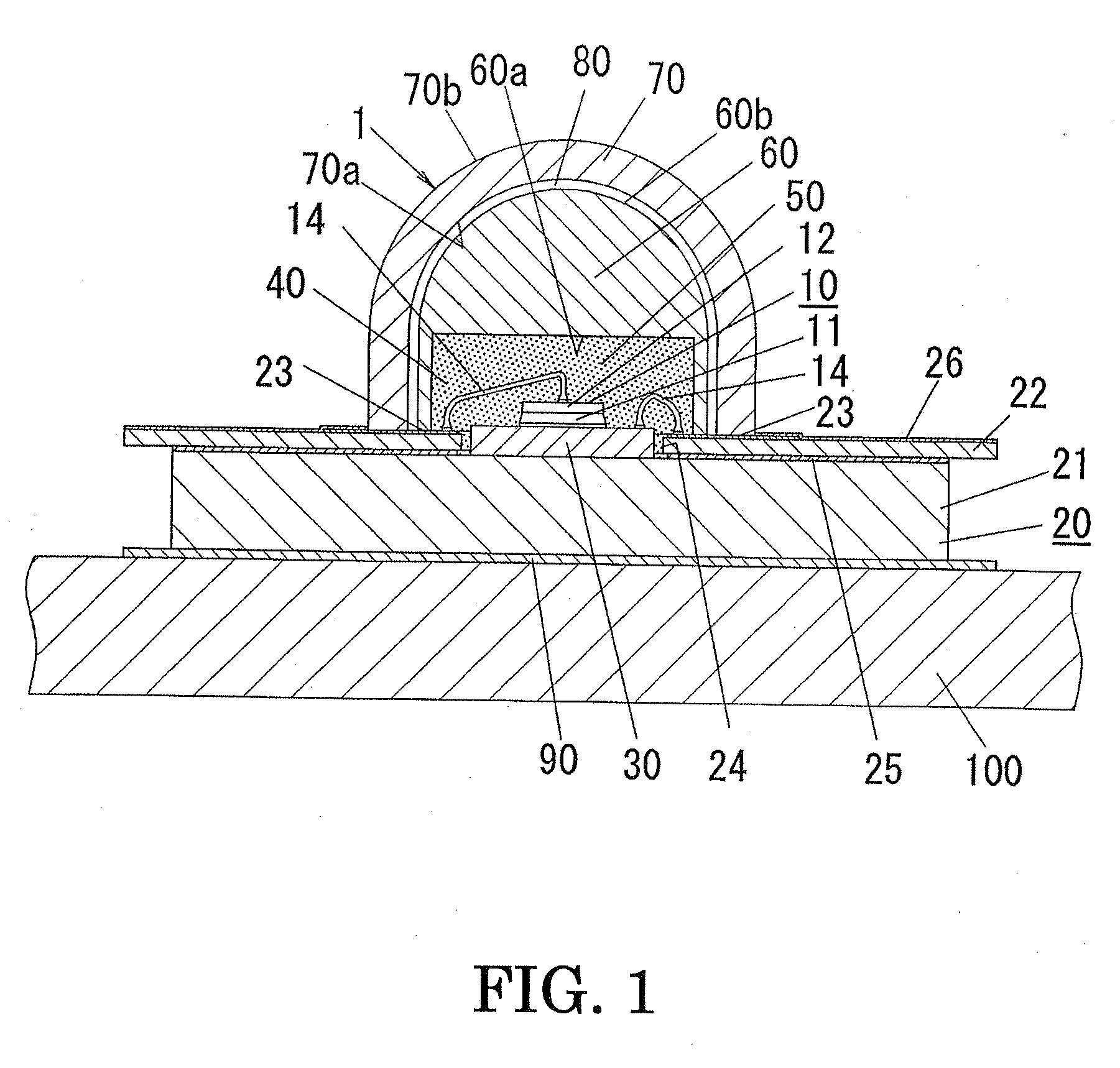
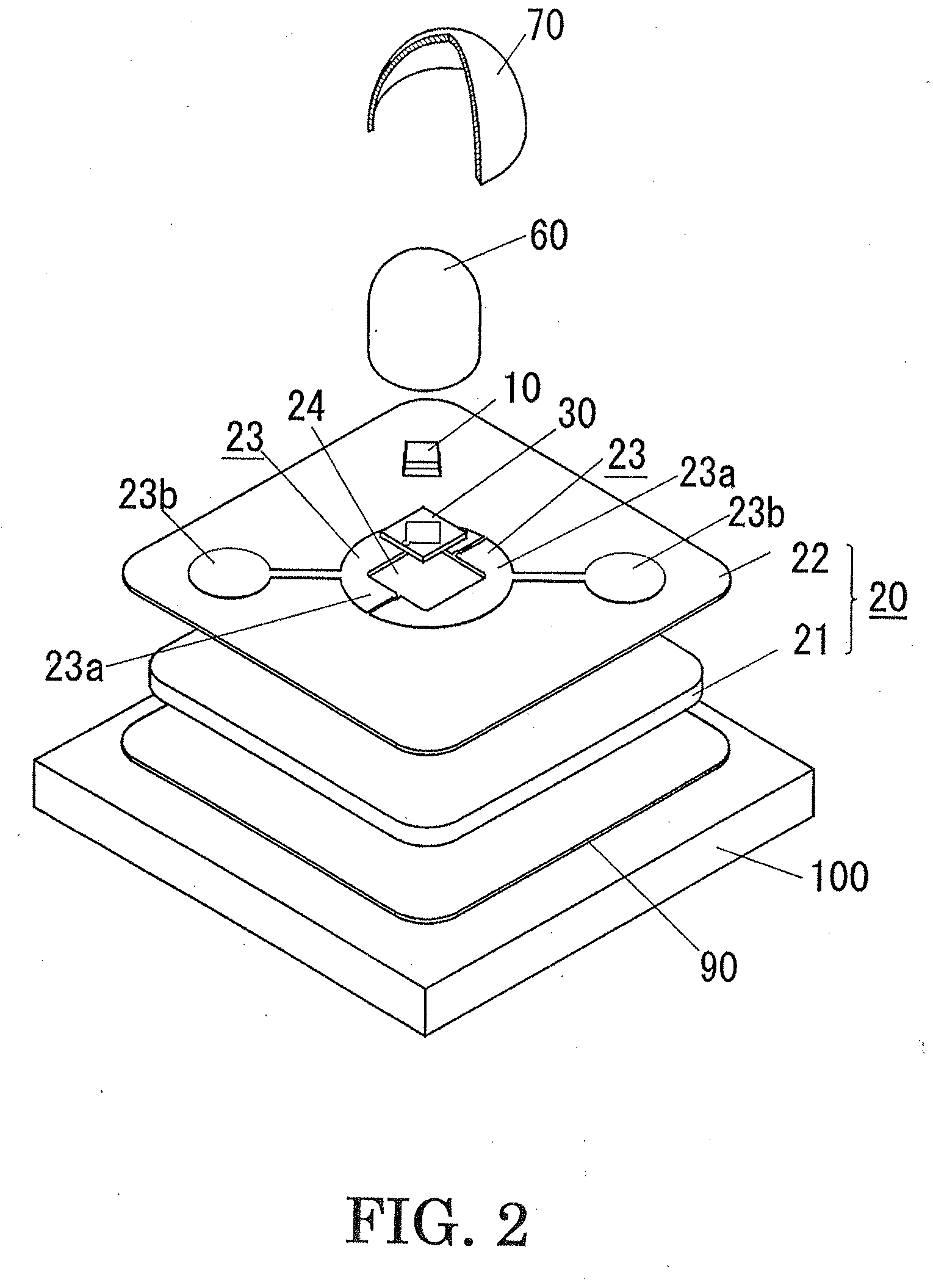
[0046]As shown in FIGS. 1 to 3, the light emitting device 1 of the present embodiment includes an LED chip 10, a mounting substrate 20 to which the LED chip 10 is mounted, an encapsulation member 50 which is elastic and formed of an encapsulation resin material to encapsulate the LED chip 10 and bonding wires 14 connected to the LED chip 10, a lens 60 formed of a transparent resin material, a dome-shaped color conversion member 70 mounted on the mounting substrate 20 to cover a light output surface 60b of the lens 60. The color conversion member 70 is molded from a transparent material and a fluorescent material which is excited by a light from the LED chip 10 to emit a light of a color different from a luminescent color of the LED chip 10. The lens 60 has a recess 40 facing a surface of the mounting substrate 20, and is fixed on the mounting substrate 20 such that the encapsulation member 50 is set into the recess 40. The color conversion member 70 is arranged to cover the lens 60 ...

second embodiment

[0075]The light emitting device 1 of this embodiment shown in FIG. 10 is almost consistent in fundamental component with that of first embodiment. Like components are designated by like reference numerals, and no duplicate explanation deemed necessary.

[0076]In this embodiment, the inner diameter of the circular-shaped opening 26a formed in a center part of the resist layer 26 is set slightly smaller than the maximum of inner diameter of the color conversion member 70, the color conversion member 70 is mounted on the mounting substrate 20 with its entire circumference joined to the periphery of circular-shaped opening 26a by an adhesive agent 75.

[0077]The manufacturing method of the light emitting device 1 in this embodiment includes the following steps. Firstly, the LED chip 10 is mounted to the mounting substrate 20, and the LED chip 10 is connected to the mounting substrate 20 by means of the bonding wires 14, as shown in FIG. 11, and then the LED chip 10 and the bonding wires 14 ...

third embodiment

[0079]The light emitting device 1 of this embodiment shown in FIG. 10 is almost consistent in fundamental component with that of first embodiment. Like parts are designated by like reference numerals, and no duplicate explanation deemed necessary.

[0080]In this embodiment, the lens 60 is provided with an injection port 41 for injecting the encapsulating resin material into the recess 40, and a discharge port 42 for discharging a residue of said encapsulating resin material.

[0081]The manufacturing method of the light emitting device 1 in this embodiment includes the following steps. At first, LED chip 10 is mounted to the mounting substrate 20 and connected to mounting substrate 20 with bonding wires 14. Then, the lens 60 is adhered to the mounting substrate 20 to dispose the LED chip 10 and bonding wires 14 within the recess 40 of the lens (step (a)). Secondly, the recess 40 of the lens is filled with the uncured encapsulation resin material through the injection port 41 of the lens ...


PUM


Abstract

The lighting device (1) includes an LED chip (10), a mounting substrate (20) mounting thereto the LED chip, an encapsulation member (50) made of an encapsulating resin material for encapsulation of the LED chip, and a lens (60) made of a transparent resin material. The lens (60) is provided in its bottom with a recess (40) and is secured to the mounting substrate (20) with the encapsulation member (50) disposed within the recess (40). The encapsulation member (50) is confined within the recess of the lens of the transparent resin material, which minimizes a difference in the coefficient of linear expansion between the encapsulation member and the surroundings for restraining occurrence of voids in the encapsulation member at a low temperature.

Description

TECHNICAL FIELD[0001]The invention relates to a light emitting device using an LED (Light Emitting Diode) chip and a fabrication method thereof.BACKGROUND ART[0002]Japanese Unexamined Patent Application Publication No. 2001-85748 (hereinafter referred to as patent document 1) and Japanese Unexamined Patent Application Publication No. 2001-148514 (hereinafter referred to as patent document 2) propose a light emitting device which comprises an LED chip, a circuit board mounting the LED chip, a metal frame (e.g. made of aluminum) surrounding the LED chip on a surface of the circuit board, and an encapsulation member (e.g. made of a transparent resin such as an epoxy resin and a silicone resin) filled within the frame to encapsulate the LED chip and bonding wires connected to the LED chip. The frame disclosed in the Patent document 1 and 2 is shaped to have an opening area which becomes greater as it is spaced further away from the circuit board and is finished to have a mirror interior...

Claims


Application Information

Patent Timeline
IPC IPC(8): H01L33/00H01L21/50H01L33/32H01L33/50H01L33/56H01L33/58H01L33/62
CPCH01L33/52H01L2924/19107H01L2224/73265H01L33/58H01L2924/181H01L2924/00012
Inventor MASUI, MIKIOURANO, YOUJI
Owner PANASONIC CORP
Learn More