Stacked semiconductor package without reduction in stata storage capacity and method for manufacturing the same

Inactive Publication Date: 2009-04-16
SK HYNIX INC
View PDF11 Cites 21 Cited by
  • Summary
  • Abstract
  • Description
  • Claims
  • Application Information

AI Technical Summary

Benefits of technology

[0009]It is an object of the present invention to provide an improved structure for a stacked semiconductor pa

Problems solved by technology

During the manufacturing process of the stacked semiconductor package, when the through electrodes (which penetrating through each semiconductor chip) are formed they occupy space, which c

Method used


Image

  • Stacked semiconductor package without reduction in stata storage capacity and method for manufacturing the same
  • Stacked semiconductor package without reduction in stata storage capacity and method for manufacturing the same
  • Stacked semiconductor package without reduction in stata storage capacity and method for manufacturing the same

Examples


Example

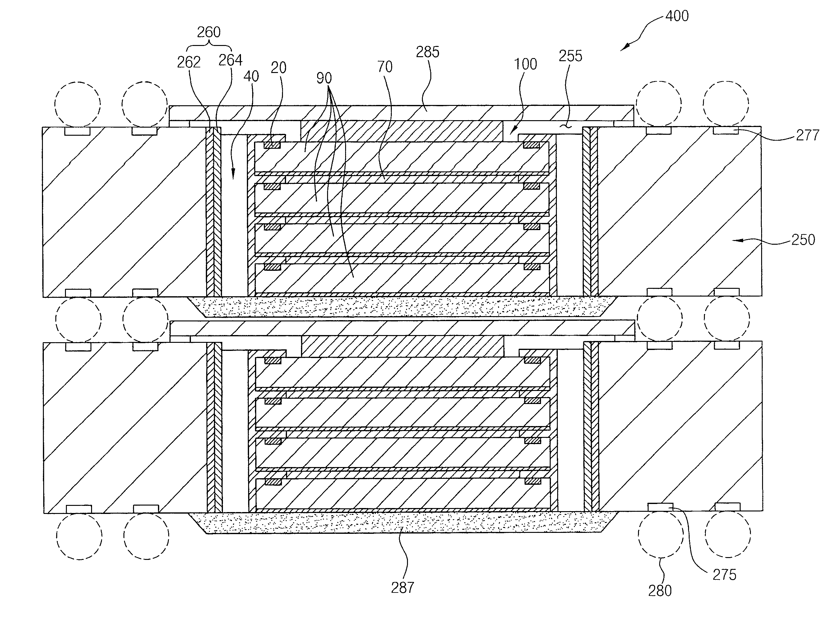
[0036]FIG. 1 is a partial cut perspective view showing a stacked semiconductor package according to an embodiment of the present invention.

[0037]Referring to FIG. 1, a stacked semiconductor package 400 comprises semiconductor chip module 100 and a substrate 200. The stacked semiconductor package 400 additionally comprises a molding member 300.

[0038]The semiconductor chip module 100 comprises at least two semiconductor chips 90 stacked on each other. As an example, in the embodiment shown in FIG. 1, the semiconductor chip module 100 comprises four semiconductor chips 90.

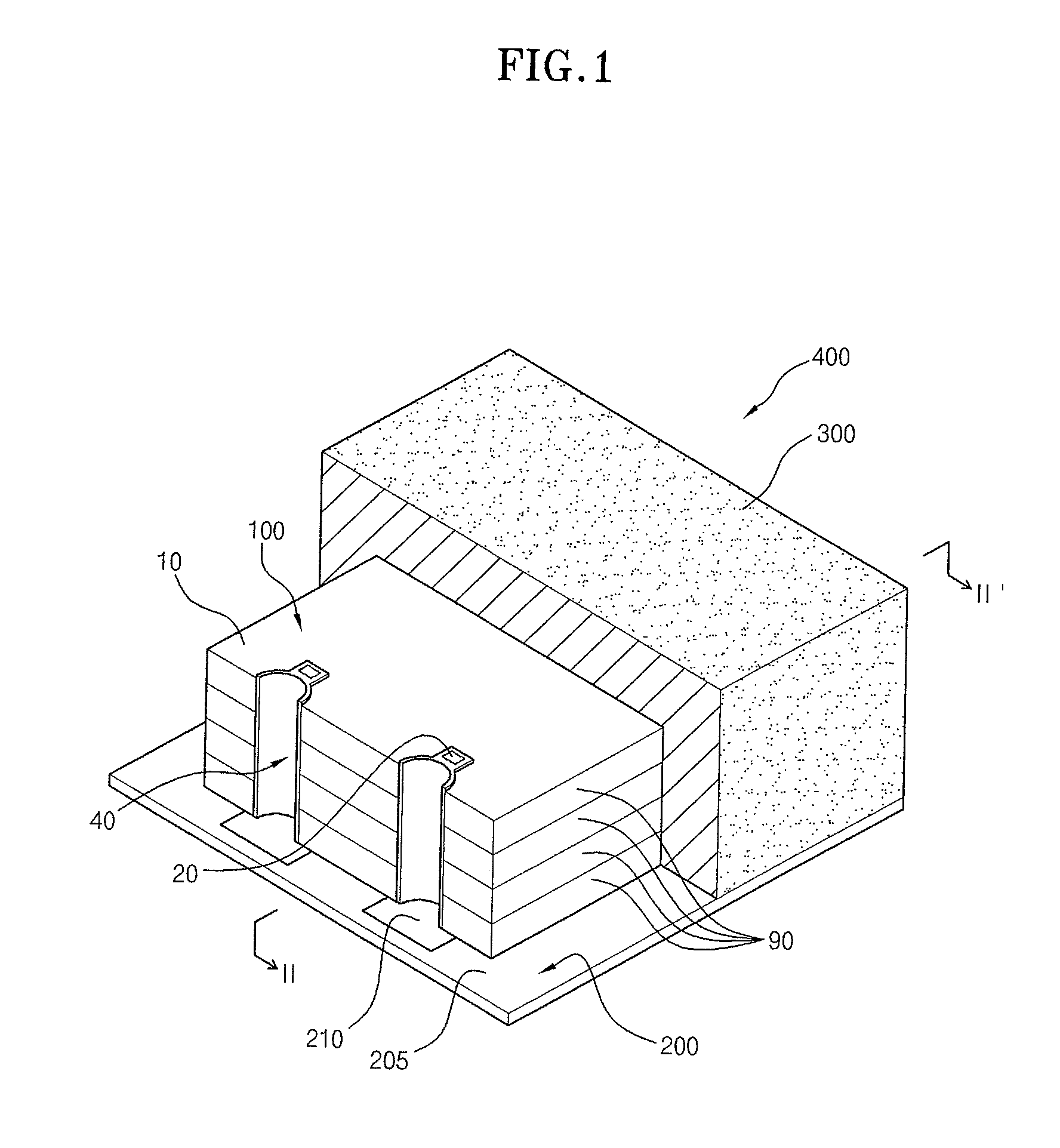
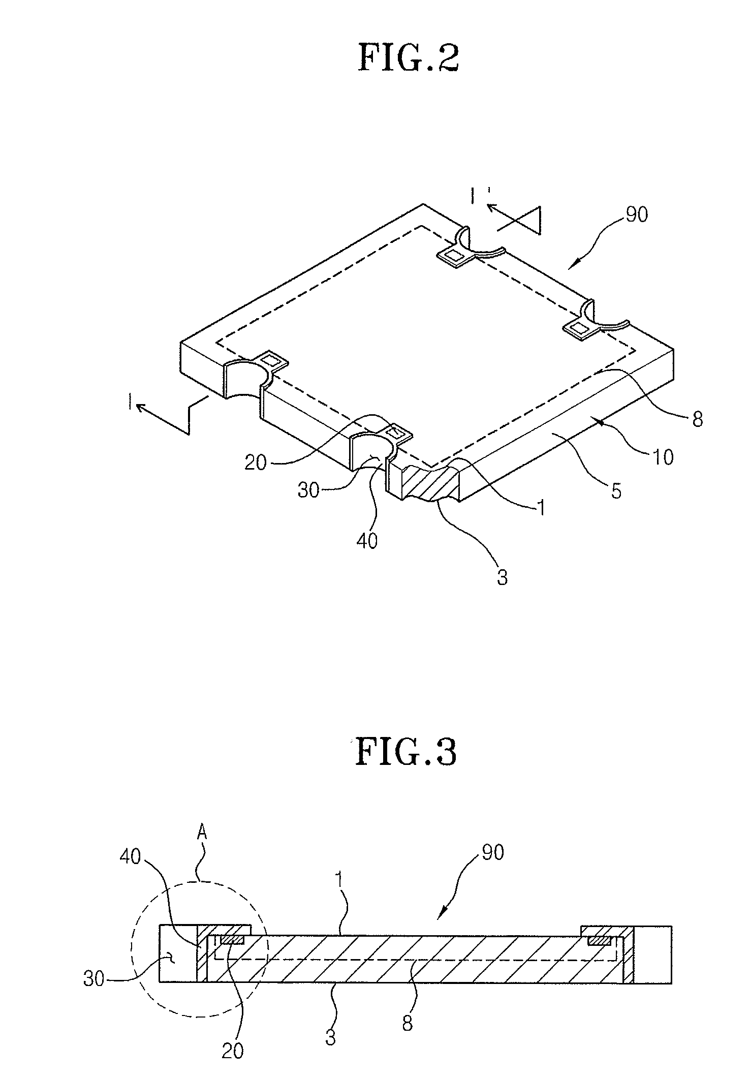
[0039]FIG. 2 is a partial cut perspective view showing any one of the semiconductor chips among the semiconductor chip modules shown in FIG. 1. FIG. 3 is a cross-sectional view taken along line I-I′ of FIG. 2. FIG. 4 is a partial enlarged view of a portion ‘A’ of FIG. 3.

[0040]Referring to FIGS. 2 and 3, each semiconductor chip 90 of the semiconductor chip module 100 comprises a semiconductor chip body 10, pads 20, rec...


PUM


Abstract

A stacked semiconductor package includes a semiconductor chip module including at least two semiconductor chips with a semiconductor chip body having an upper surface, a lower surface, side surfaces coupling the upper surface and the lower surface, and a circuit part. The semiconductor chips include pads coupled to the circuit part and disposed at an edge of the upper surface. A recess parts are concavely formed in the side surfaces corresponding to each pad. Conductive connection patterns cover the recess parts, and each conductive connection pattern is electrically connected to a corresponding bonding pad. The semiconductor chip module is disposed on a substrate, and the contact pads of the semiconductor substrate are electrically connected to the conductive connection patterns. The stacked semiconductor package provides an improved structure that can contain a plurality of stacked semiconductor chips with no reduction in data storage capacity.

Description

CROSS-REFERENCE TO RELATED APPLICATIONS[0001]The present application claims priority to Korean patent application number 10-2007-0103881 filed on Oct. 16, 2007 and 10-2007-0106480 filed on Oct. 23, 2007, which are incorporated herein by reference in its entirety.BACKGROUND OF THE INVENTION[0002]The present invention relates to a stacked semiconductor package and a method for manufacturing the same, and more particularly to a stacked semiconductor package having an improved structure which prevents a reduction in data storage capacity.[0003]Recent developments in semiconductor manufacturing technology have lead to the development of various types of semiconductor packages with semiconductor devices suitable for processing more data within a short time.[0004]A semiconductor package is typically manufactured through a semiconductor chip manufacturing process that manufactures semiconductor chips including semiconductor devices on a wafer made of high purity silicon, a die sorting proce...

Claims


Application Information

Patent Timeline
IPC IPC(8): H01L21/50H01L23/02
CPCH01L23/3128H01L25/0657H01L25/105H01L2225/1058H01L2225/06551H01L2225/1035H01L2224/24145
Inventor JUNG, YOUNG HY
Owner SK HYNIX INC
Why Eureka
Try Eureka