Differential amplification circuit and manufacturing method thereof

a technology of amplification circuit and manufacturing method, which is applied in the direction of amplification control details, testing electric installations on transport, instruments, etc., can solve the problems of disadvantageous compounding of above-described errors, and achieve the effect of preventing the occurrence of potential-dependent errors

Inactive Publication Date: 2009-04-16
DENSO CORP
View PDF4 Cites 3 Cited by
  • Summary
  • Abstract
  • Description
  • Claims
  • Application Information

AI Technical Summary

Benefits of technology

[0020]Consequently, when the differential amplification circuit is incorporated in the system shown in FIG. 24, even if the potentials at the terminals of the shunt resistor 67 fluctuate due to the wiring resistors, the offset voltage of the differential amplification circuit will not fluctuate along with the fluctuation in the potentials. In other words, since the resistance value of any of the resistors 1 to 4 is adjusted so that the offset voltage will be corrected, occurrence of a potential-dependent error derived from a variance in resistances in the differential amplification circuit can be prevented. Even when the voltage across the terminals of the battery 60 is measured, occurrence of a potential-dependent error can be prevented.
[0029]Consequently, since the resistance varying means 20, 30, 40, 40′; or 50 can be realized with a fixed resistor devoid of a moving element included in a potentiometer or the like, the differential amplification circuit can be readily incorporated in an IC. Moreover, since the resistance varying means 20, 30, 40, 40, or 50 is realized with a fixed resistor and devoid of a sliding element, the reliability of the resistance varying means 20, 30, 40, 40, or 50 can be improved. Moreover, the employment of a digital signal permits electrical high-speed adjustment. Eventually, the mass-productivity of the differential amplification circuit can be improved.
[0031]When a configuration employing the analog multiplexer 42 or 42′ is adopted as that of the resistance varying means 20, 30, 40, 40′, or 50 and the pieces of switch means 34 are connected to the inverting input terminal and non-inverting input terminal of the operational amplifier 10 capable of ignoring a flowing current, a potential drop caused by a resistance introduced by the pieces of switch means 34 can be ignored. Consequently, highly precise adjustment can be achieved.
[0033]What is referred to as a resolution is the smallest changeable step by which a differential amplification circuit output can be changed by the resistance varying means 40 or 40′. When the configuration including the two pieces of resistance varying means 40 and 40′ is adopted, the number of adjustment steps for a resistance value permitted in the differential amplification circuit is a product of the number of steps, which is supported by one of the pieces of resistance varying means, by the number of steps supported by the other resistance varying means. Consequently, the differential amplification circuit can be constructed using a small number of resistors and a small number of switches.

Problems solved by technology

Thus, the above described error can be disadvantageously compounded.

Method used


Image

  • Differential amplification circuit and manufacturing method thereof
  • Differential amplification circuit and manufacturing method thereof
  • Differential amplification circuit and manufacturing method thereof

Examples


first embodiment

[0062]The first embodiment of the invention will be described below with reference to the drawings.

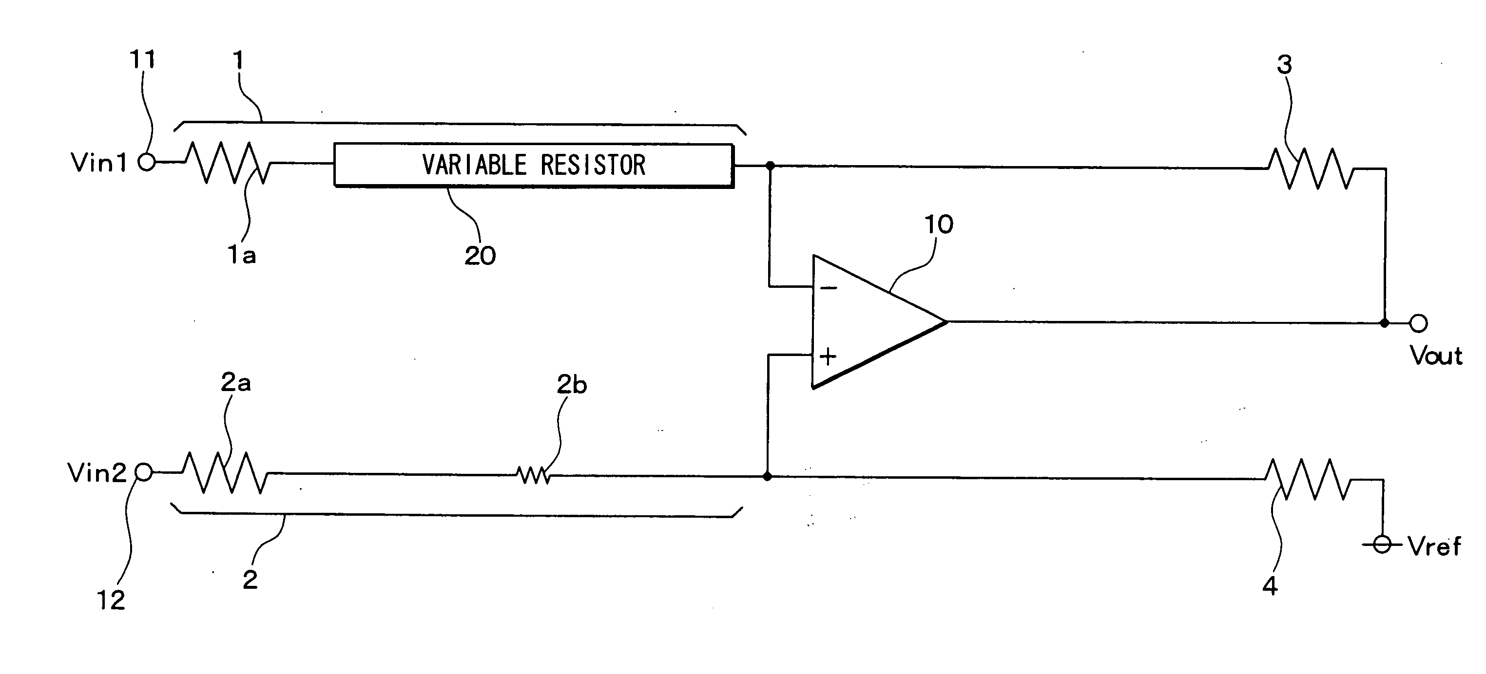
[0063]FIG. 1 is a circuit diagram of a differential amplification circuit in accordance with a first embodiment. As shown in the drawing, the difference amplification circuit includes a first resistor 1, a second resistor 2, a third resistor 3, a fourth resistor 4, and an operational amplifier 10.

[0064]The first resistor 1 is connected between a first input terminal 11 brought to a first input potential Vin1 and an inverting input terminal of the operational amplifier 10, and functions as an input resistor. The second resistor 2 is connected between a second input terminal 12 brought to a second input potential Vin2 and a non-inverting input terminal of the operational amplifier 10, and functions as an input resistor. The third resistor 3 is connected between the inverting input terminal of the operational amplifier 10 and the output terminal of the operational amplifier 10. The fourth...

second embodiment

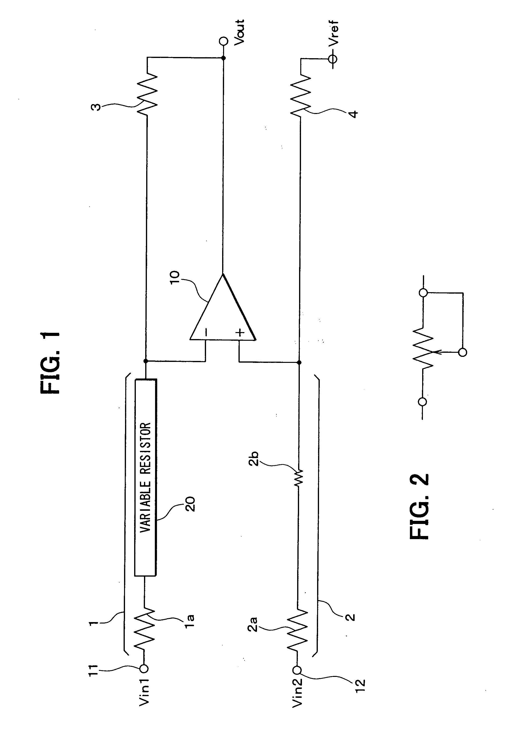
[0087]A second embodiment will be described focusing primarily on differences from a first embodiment. FIG. 3 is a circuit diagram of a differential amplification circuit in accordance with the present embodiment. As shown in the drawing, a first resistor 1 includes a fixed resistor 1a and a dummy resistor 1b, and a second resistor 2 includes a fixed resistor 2a and a variable resistor 20.

[0088]In the present embodiment, the resistance value of the second resistor 2 among the resistors 1 to 4 is adjusted in order to correct the offset voltage of the differential amplification circuit. Thus, the resistance value of the variable resistor 20 included in the second resistor 2 may be adjusted.

third embodiment

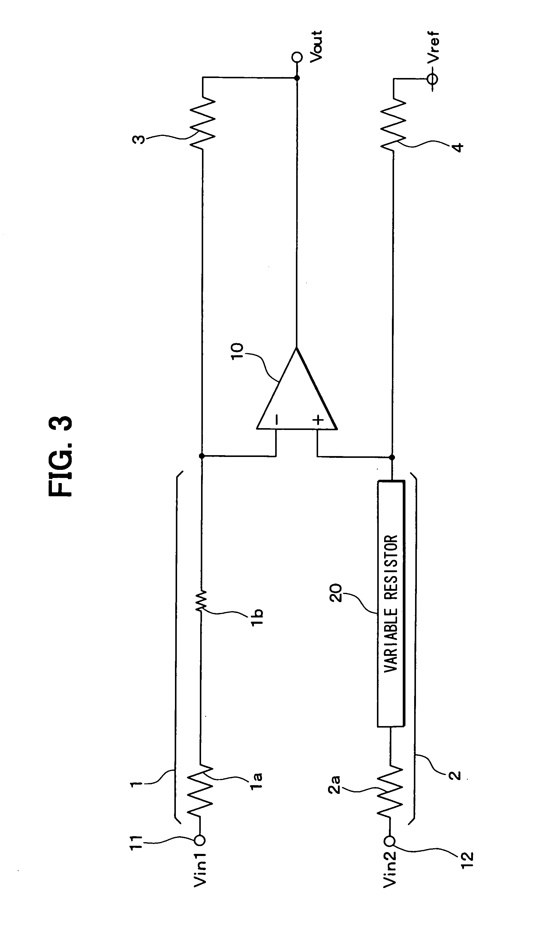
[0089]A third embodiment will be described focusing primarily on differences from a first and second embodiment. FIG. 4 is a circuit diagram of a differential amplification circuit in accordance with the present embodiment. As shown in the drawing, a third resistor 3 includes a fixed resistor 3a and a variable resistor 20, and a fourth resistor 4 includes a fixed resistor 4a and a dummy resistor 4b. Thus, the circuit form in which the resistance value of the variable resistor 20 included in the third resistor 3 is adjusted will satisfactorily provide the ability for adjustment.


PUM


Abstract

A differential amplification circuit and a method corrects an offset voltage derived from a variance in resistances. With first and second input terminals brought to the same potential and set to a potential different from a reference potential, the resistance value of resistors is adjusted so that an output potential and the reference potential will be substantially equal to each other.

Description

CROSS REFERENCE TO RELATED APPLICATIONS[0001]The present application is based on and claims priority to Japanese Patent Applications No. 2007 268133 filed Oct. 15, 2007, the entire contents of which are incorporated herein by reference.BACKGROUND OF THE INVENTION[0002]1. Field of the Invention[0003]The invention relates to a differential amplification circuit compensating for an offset voltage from a variance in resistances, and a manufacturing method.[0004]2. Description of the Related Art[0005]In the past, a current detection device including a shunt resistor that detects a current flowing into a battery, an amplifier that amplifies a voltage across the terminals of the shunt resistor, and a switch that is used to strap two input terminals of the amplifier so as to temporary bring an input voltage to a zero or near zero value as been proposed. Refer, for example, to JP-A-2006-64627 where such an amplifier encompassing a differential amplification circuit is described.[0006]In a pr...

Claims


Application Information

Patent Timeline
Patent Type & Authority Applications(United States)
IPC IPC(8): H03F3/45
CPCG01R1/203H03G1/0088G01R19/0092G01R31/006H03F3/45475H03F3/45928H03F2200/261H03F2200/462H03F2200/471H03F2203/45101H03F2203/45138H03F2203/45522H03F2203/45528H03F2203/45586H03F2203/45588H03F2203/45591H03F2203/45594G01R19/0023
Inventor TANIZAWA, YUKIHIKO
Owner DENSO CORP
Why Eureka
Try Eureka