Semiconductor Device

a technology of semiconductor devices and semiconductors, applied in semiconductor devices, semiconductor/solid-state device details, electrical apparatus, etc., can solve the problems of difficult deformation of the flow direction of the conductor provided on the sheet-form wiring member, and achieve the effect of reducing the manufacturing yield, facilitating semiconductor devices, and facilitating reliability

Active Publication Date: 2009-04-23
ROHM CO LTD
View PDF11 Cites 12 Cited by
  • Summary
  • Abstract
  • Description
  • Claims
  • Application Information

AI Technical Summary

Benefits of technology

[0016]Preferably, the semiconductor device in accordance with the above-described aspect of the present invention is structured such that the upper surfaces of the one end portions of the lead terminals are at substantially a same height as the surface on the one side of the semiconductor chip. With this structure, the electrodes of the semiconductor chip and the one end portions of the lead terminals can be electrically connected respectively to each other with more ease. Consequently, it is possible to cope with even larger numbers of pins and even finer pitches while suppressing the lowering of the manufacturing yield and reliability with more ease.
[0017]Preferably, the semiconductor device in accordance with the above-described aspect of the present invention is formed into the QFP type package by sealing the semiconductor chip in the sealing-resin layer. This structure makes it possible to easily obtain semiconductor devices that can cope with larger numbers of pins and finer pitches while suppressing the lowering of the manufacturing yield and reliability of the semiconductor devices.
[0018]As described above, according to the present invention, it is possible to easily obtain semiconductor devices that can cope with even larger numbers of pins and even finer pitches while suppressing the lowering of the manufacturing yield and reliability of the semiconductor devices.

Problems solved by technology

That is, during the process of resin-sealing the semiconductor chip with the sealing-resin layer, the conductors provided on the sheet-form wiring member are difficult to deform in the flow direction of the sealing resin as compared with the bonding wires.

Method used


Image

  • Semiconductor Device
  • Semiconductor Device
  • Semiconductor Device

Examples


Embodiment Construction

[0029]A preferred embodiment of the present invention will be described in detail below with reference to the accompanying drawings. This embodiment deals with a case where the present invention is applied to a QFP type semiconductor device as an example of resin-sealed type semiconductor devices.

[0030]First, with reference to FIGS. 1 to 5, a structure of a semiconductor device in accordance with one embodiment of the present invention will be described.

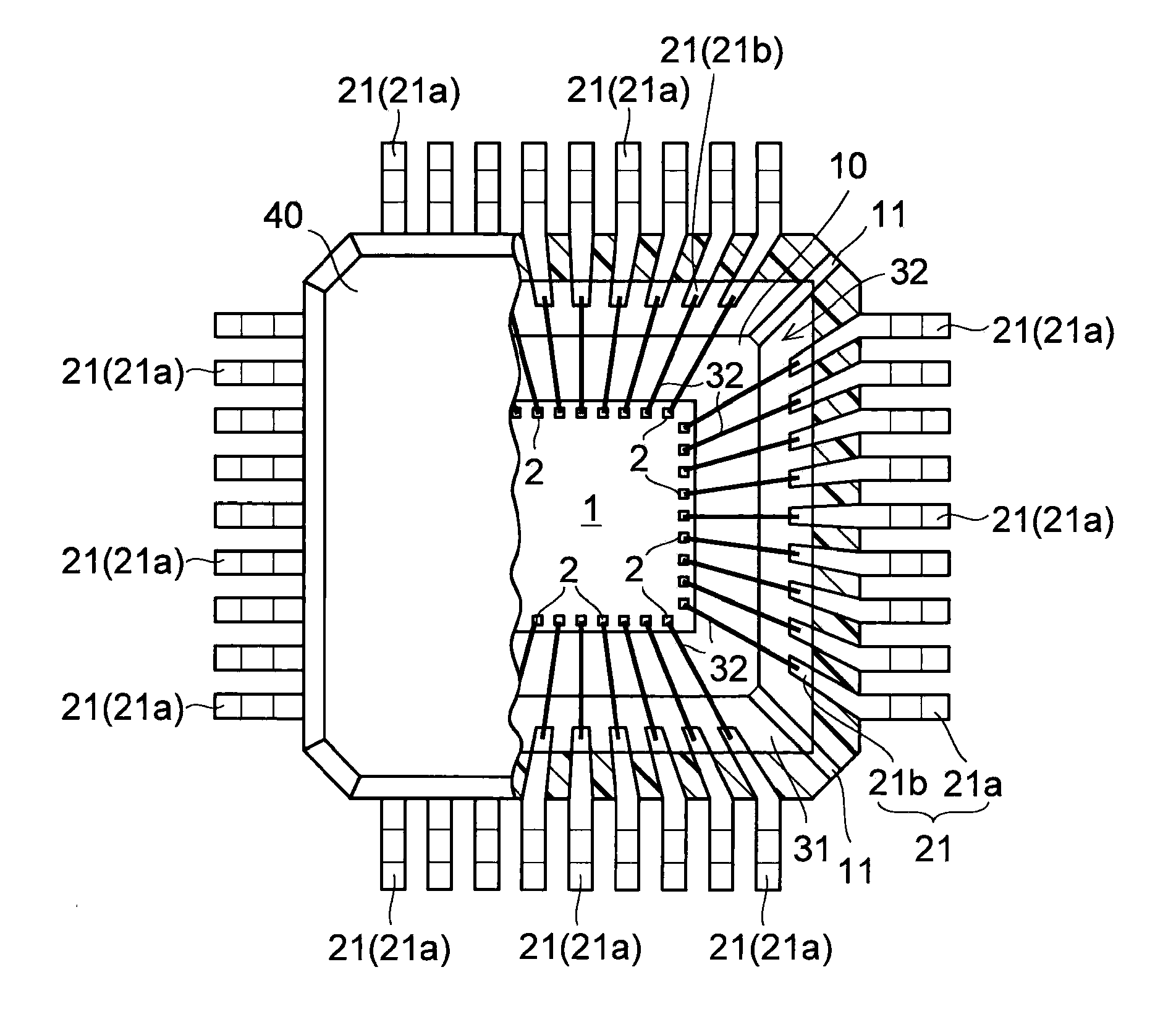
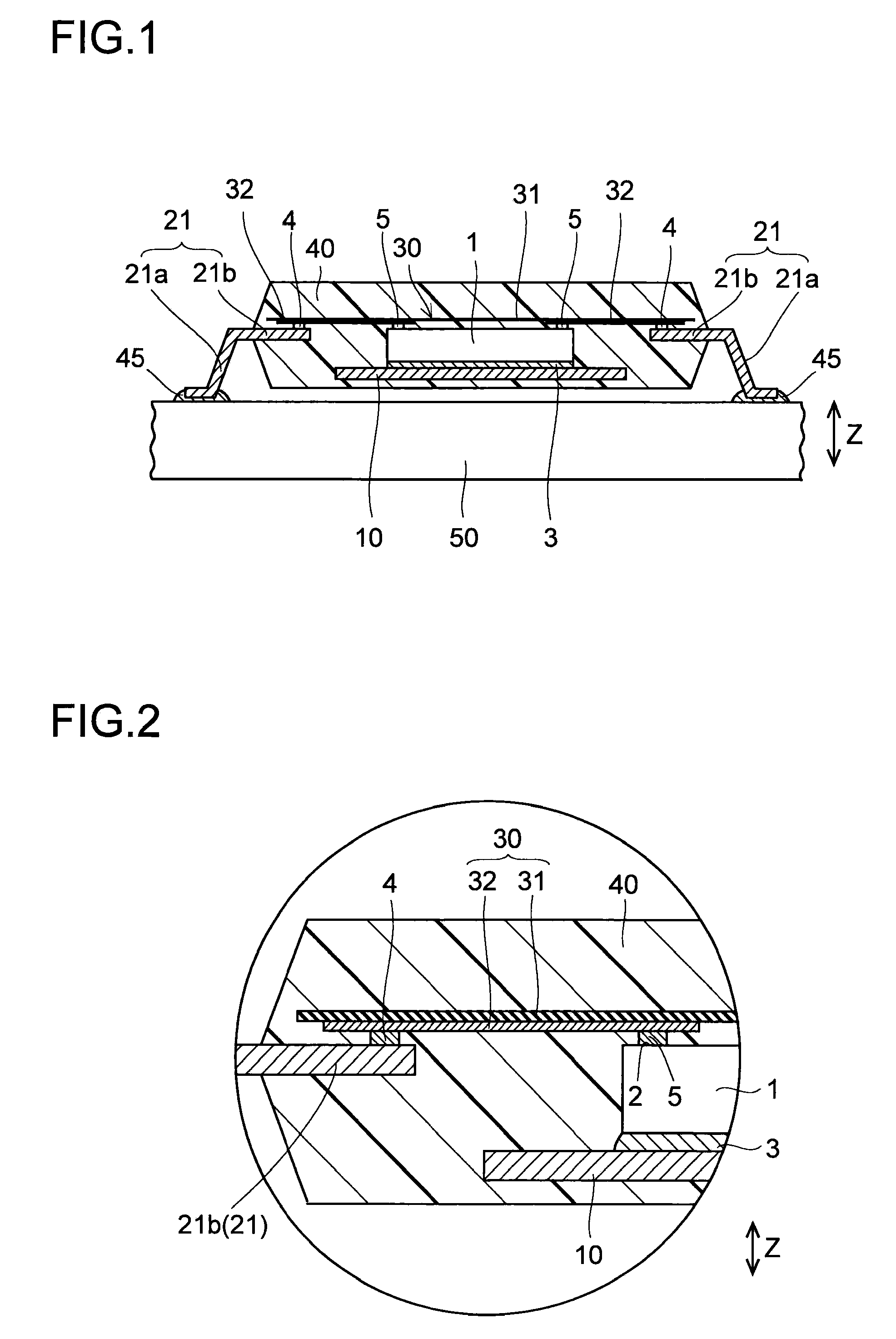
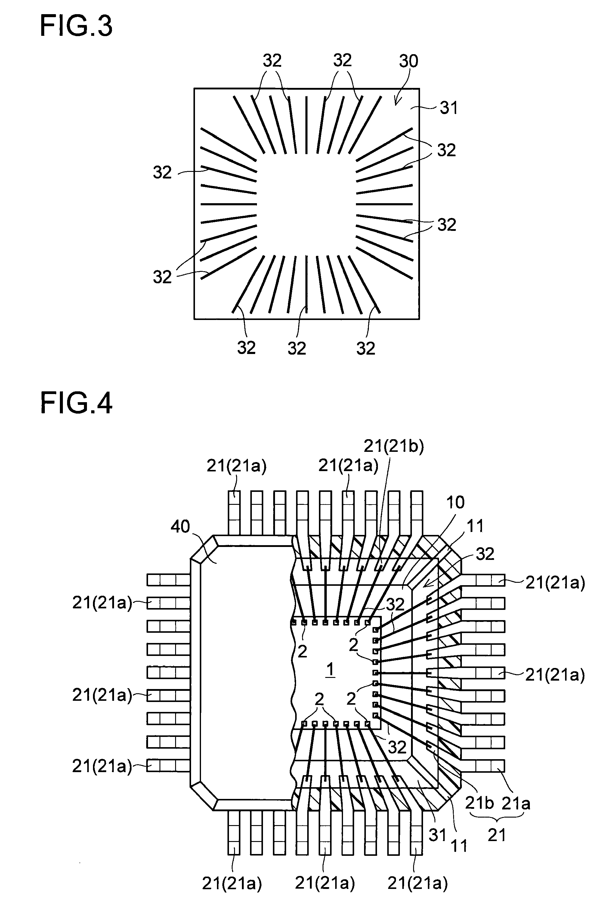
[0031]As shown in FIG. 1, the semiconductor device in accordance with the one embodiment of the present invention includes: a semiconductor chip 1; a die pad 10 having the semiconductor chip 1 mounted thereon; a plurality of lead terminals 21; a sheet-form wiring member 30 for electrically connecting the semiconductor chip1 and the plurality of lead terminals 21; and a resin-sealing layer 40.

[0032]The semiconductor chip 1 includes a silicon substrate having an integrated circuit or the like formed on a main surface on one side (an up...


PUM


Abstract

A semiconductor device that can cope with larger numbers of pins and finer pitches while suppressing lowering of the manufacturing yield and reliability includes: a semiconductor chip having a plurality of electrodes provided on an upper surface thereof; a plurality of lead terminals including inner lead portions disposed toward the semiconductor chip; a sheet-form wiring member having a plurality of conductors insulated from one another on one main surface thereof; and a sealing-resin layer for sealing at least the semiconductor chip, the inner lead portions and the wiring member. The electrodes of the semiconductor device and the inner lead portions of the lead terminals are electrically connected respectively to each other via the conductors of the wiring member.

Description

[0001]This nonprovisional application claims priority under 35 U.S.C. § 119(a) on Patent Application No. 2007-272443 filed on Oct. 19, 2007, the entire contents of which are hereby incorporated by reference.BACKGROUND OF THE INVENTION[0002]1. Field of the Invention[0003]The present invention relates to semiconductor devices, and in particular to a semiconductor device of the resin-sealed type formed with a lead frame.[0004]2. Description of Related Art[0005]As an example of semiconductor devices of a resin-sealed type that are formed with a lead frame, those of a QFP (Quad Flat Package) type are conventionally known. Generally, in QFP type semiconductor devices, by narrowing the width of the inner lead portions (lead terminals) of the lead frame, larger number of pins and finer pitches are achieved so as to cope with higher degrees of integration in semiconductor elements.[0006]However, since there is a limit to the formation of the width of inner lead portions (lead terminals), in ...

Claims


Application Information

Patent Timeline
Patent Type & Authority Applications(United States)
IPC IPC(8): H01L23/495
CPCH01L23/49524H01L24/50H01L2924/01015H01L2924/01029H01L2924/01079H01L2224/32245H01L2924/01322H01L2924/14H01L2924/01006H01L2924/01033H01L2924/014H01L2924/01082H01L24/86
Inventor TADAOKA, AKIHIKO
Owner ROHM CO LTD
Why Eureka
Try Eureka