

Chip-type LED and method for manufacturing the same
- Summary
- Abstract
- Description
- Claims
- Application Information
AI Technical Summary
Benefits of technology
Problems solved by technology
Method used
Image

Examples
embodiment 1
Variation 3 of Embodiment 1
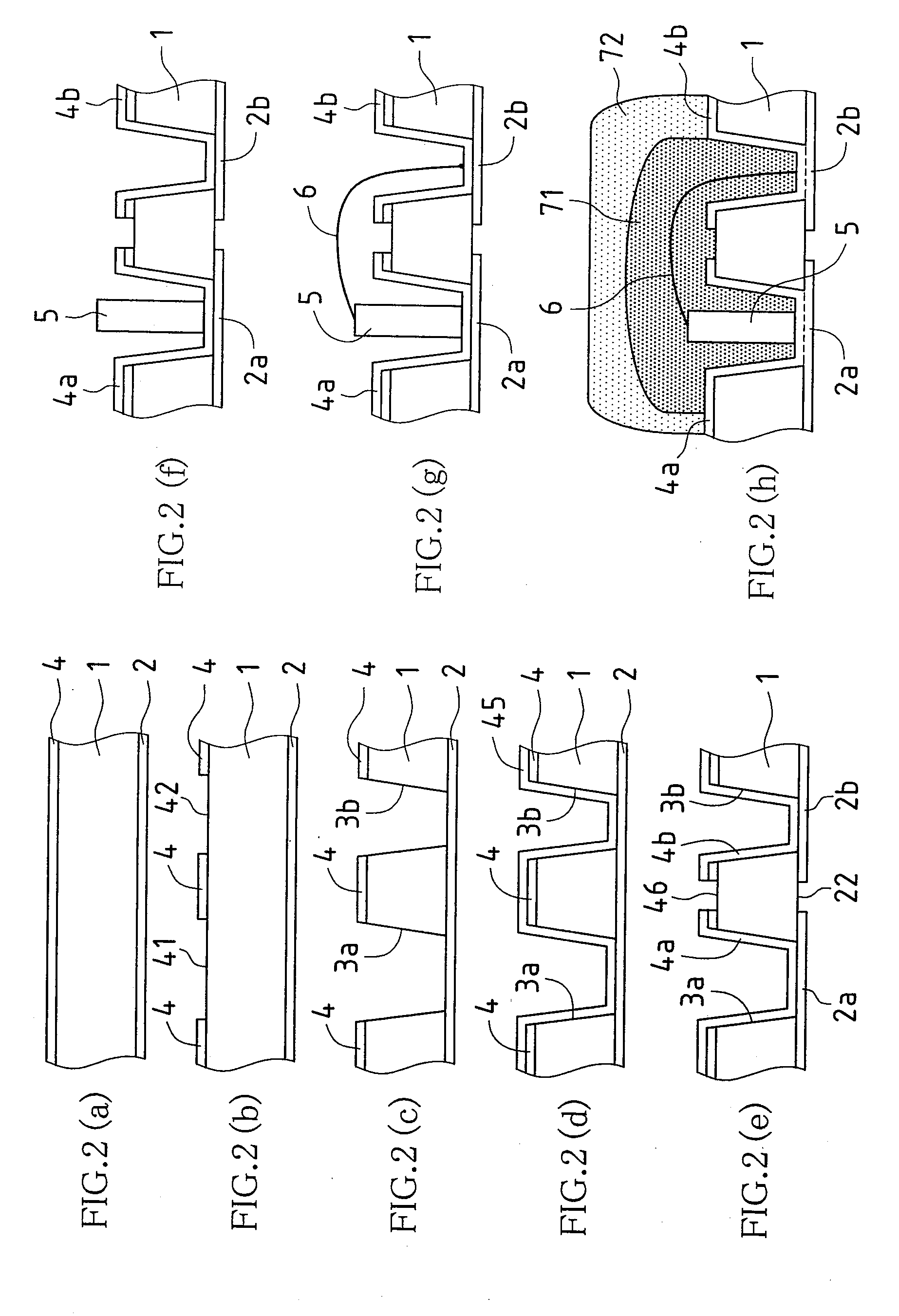
[0089]FIG. 5 is a cross-sectional view showing the structure of a chip-type LED 10 according to Variation 3 of Embodiment 1.
[0090]Variation 3 employs a structure in which the second transparent resin 72 is formed to include the entire first transparent resin 71, the entire first recess hole 3a and the periphery of the hole, and not to include the second recess hole 3b. Other elements are the same as those of the chip-type LED 10 according to Variation 1 of Embodiment 1 shown in FIG. 3, and thus a description thereof is omitted here. Similarly, a manufacturing method thereof is the same as the manufacturing method described with reference to FIGS. 2(a) to 2(h), and thus a description thereof is omitted here.
embodiment 2
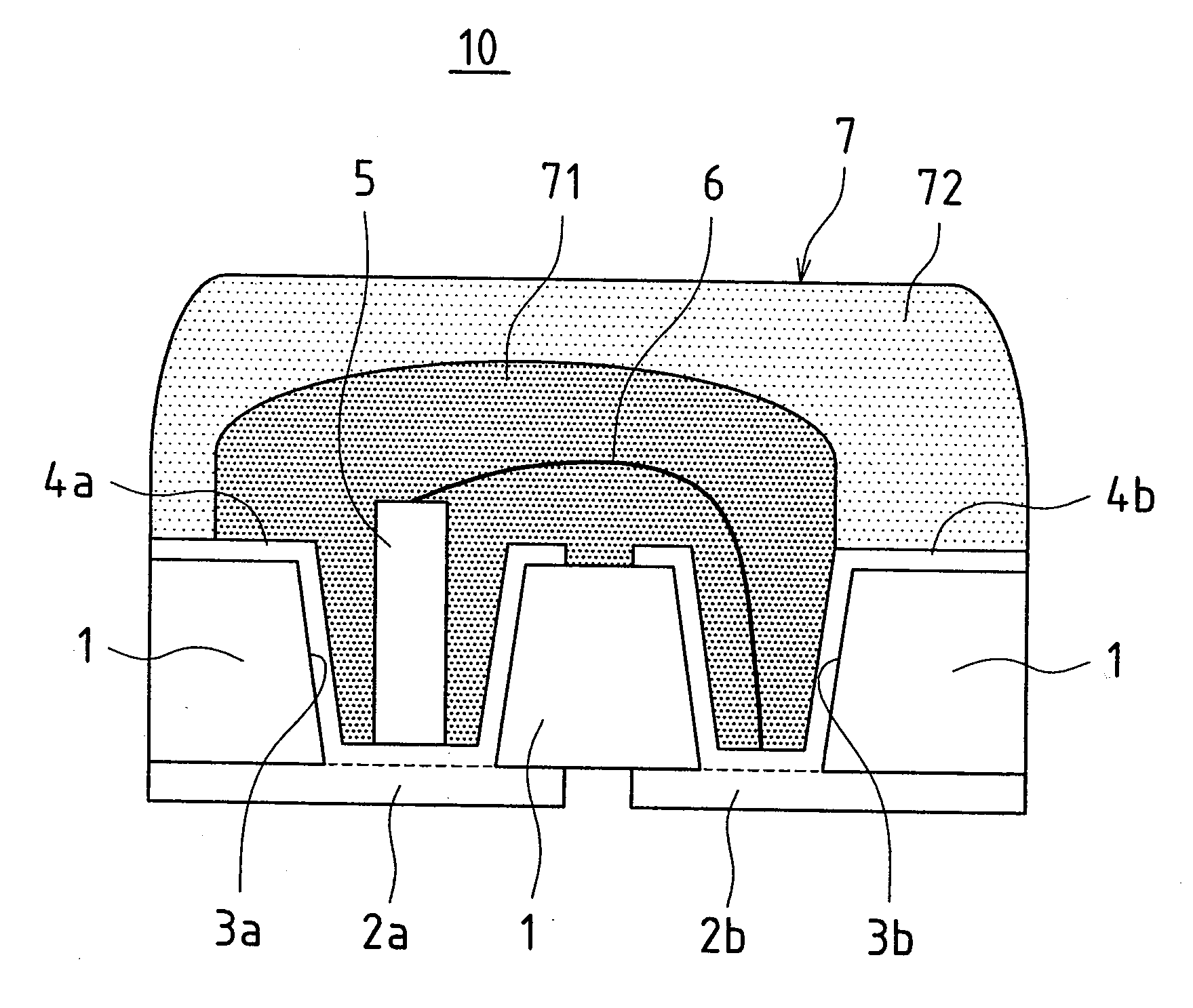
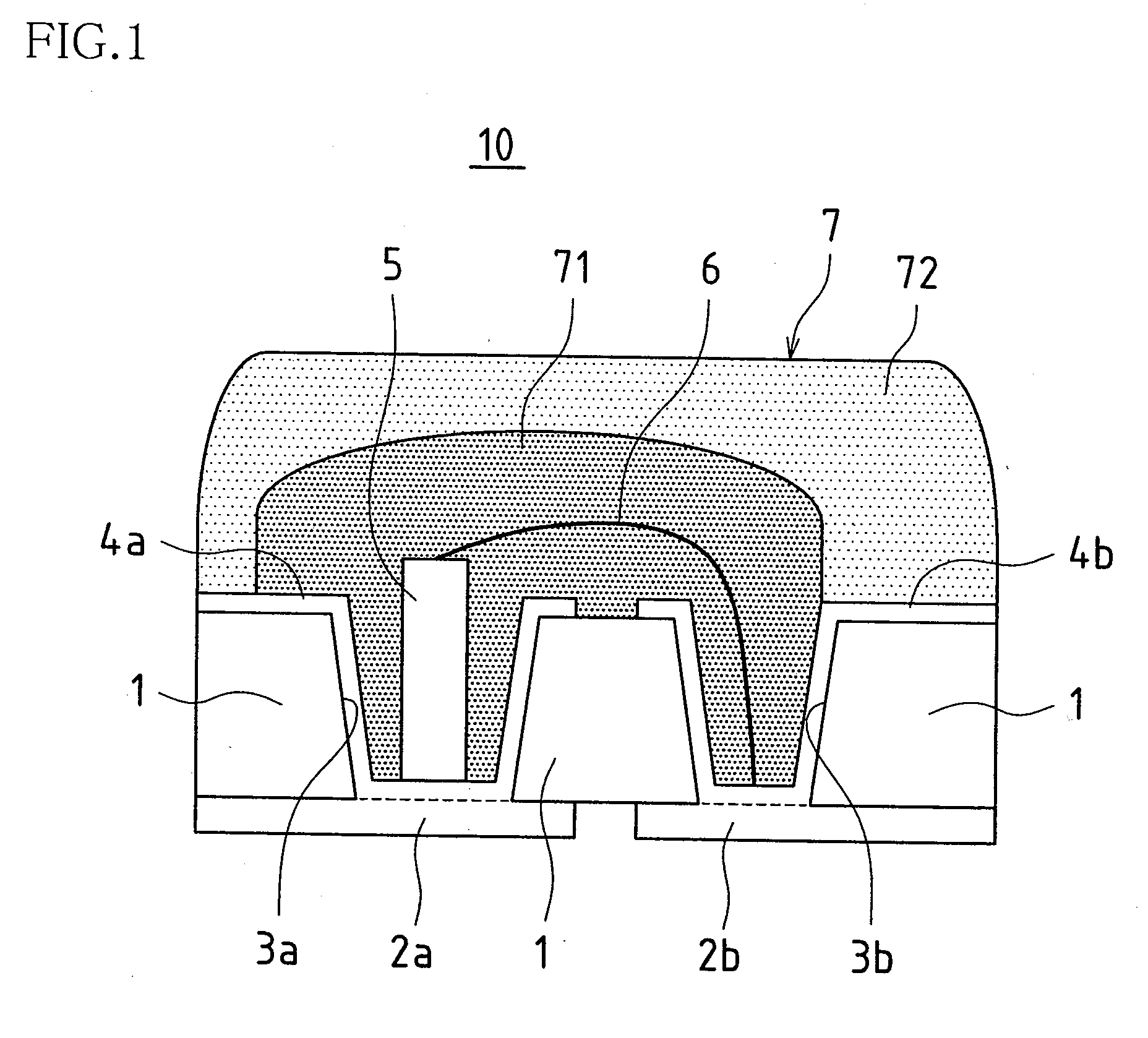
[0091]FIG. 6 is a cross-sectional view showing the structure of a chip-type LED 20 according to Embodiment 2. In the description given below, the same reference numerals are assigned to components that are the same (or have the same functions) as those of Embodiment 1 described above.
[0092]In the chip-type LED 20, a first recess hole (through hole) 3a for mounting an LED chip is formed in an insulating substrate 1. A second recess hole (through hole) 3b and a third recess hole (through hole) 3c both for connecting a fine metal wire are formed on opposite sides of the first recess hole 3a so as to sandwich the first recess hole 3a. Metal (Cu) sheets 2a, 2b and 2c serving as the wiring patterns for the recess holes are formed on the undersurface of the insulating substrate 1 in an electrically insulated state. On the surface side of the insulating substrate 1, a metal sheet 4a serving as a first wiring pattern is formed in a portion that includes the first recess hole 3a, a metal shee...
embodiment 3
Variation 1 of Embodiment 3
[0124]FIG. 11 is a cross-sectional view showing the structure of a chip-type LED 30 according to Variation 1 of Embodiment 3.
[0125]Variation 1 of Embodiment 3 employs a structure in which the first transparent resin 71 is formed to include only the entire first recess hole 3a, including the LED chip 5 and part of the fine metal wire 6 connected to the LED chip 5, and the periphery of the hole, and not to include the second recess hole 3b. Other elements are the same as those of the chip-type LED 10 of Embodiment 3 shown in FIG. 8, and thus a description thereof is omitted here. Similarly, a manufacturing method thereof is the same as the manufacturing method of Embodiment 3 described with reference to FIGS. 10(a) to 10(h), and thus a description thereof is omitted here.
[0126]Embodiments 1 to 3 given above are discussed in the context of a single-chip LED lamp that includes a pair of patterns on an insulating substrate, but it is also possible to configure ...
PUM
 Abstract
Description
Claims
Application Information