Integrated Circuit Semiconductor Device Including Stacked Level Transistors and Fabrication Method Thereof

a semiconductor device and integrated circuit technology, applied in the direction of semiconductor devices, electrical equipment, transistors, etc., can solve the problems of short channel effect and deterioration of current driving capability of cell array transistors, and achieve the effect of improving integration density and integration density

Active Publication Date: 2009-04-30
SAMSUNG ELECTRONICS CO LTD
View PDF4 Cites 164 Cited by
  • Summary
  • Abstract
  • Description
  • Claims
  • Application Information

AI Technical Summary

Benefits of technology

[0006]The present invention provides an integrated circuit semiconductor device in which a cell array transistor or a peripheral circuit transistor is configured with a vertical transistor to improve integration density, or which includes stacked vertical or planar transistors to improve the integration density.
[0007]The present invention also provides a fabrication method of an integrated circuit semiconductor device, which can achieve simplicity in fabrication when vertical or planar transistors are stacked to form a cell array transistor or a peripheral transistor on a substrate.

Problems solved by technology

The decrease in the design rule of the integrated circuit semiconductor device results in a short-channel effect and deterioration of current driving capability of the cell array transistor.

Method used


Image

  • Integrated Circuit Semiconductor Device Including Stacked Level Transistors and Fabrication Method Thereof
  • Integrated Circuit Semiconductor Device Including Stacked Level Transistors and Fabrication Method Thereof
  • Integrated Circuit Semiconductor Device Including Stacked Level Transistors and Fabrication Method Thereof

Examples


Embodiment Construction

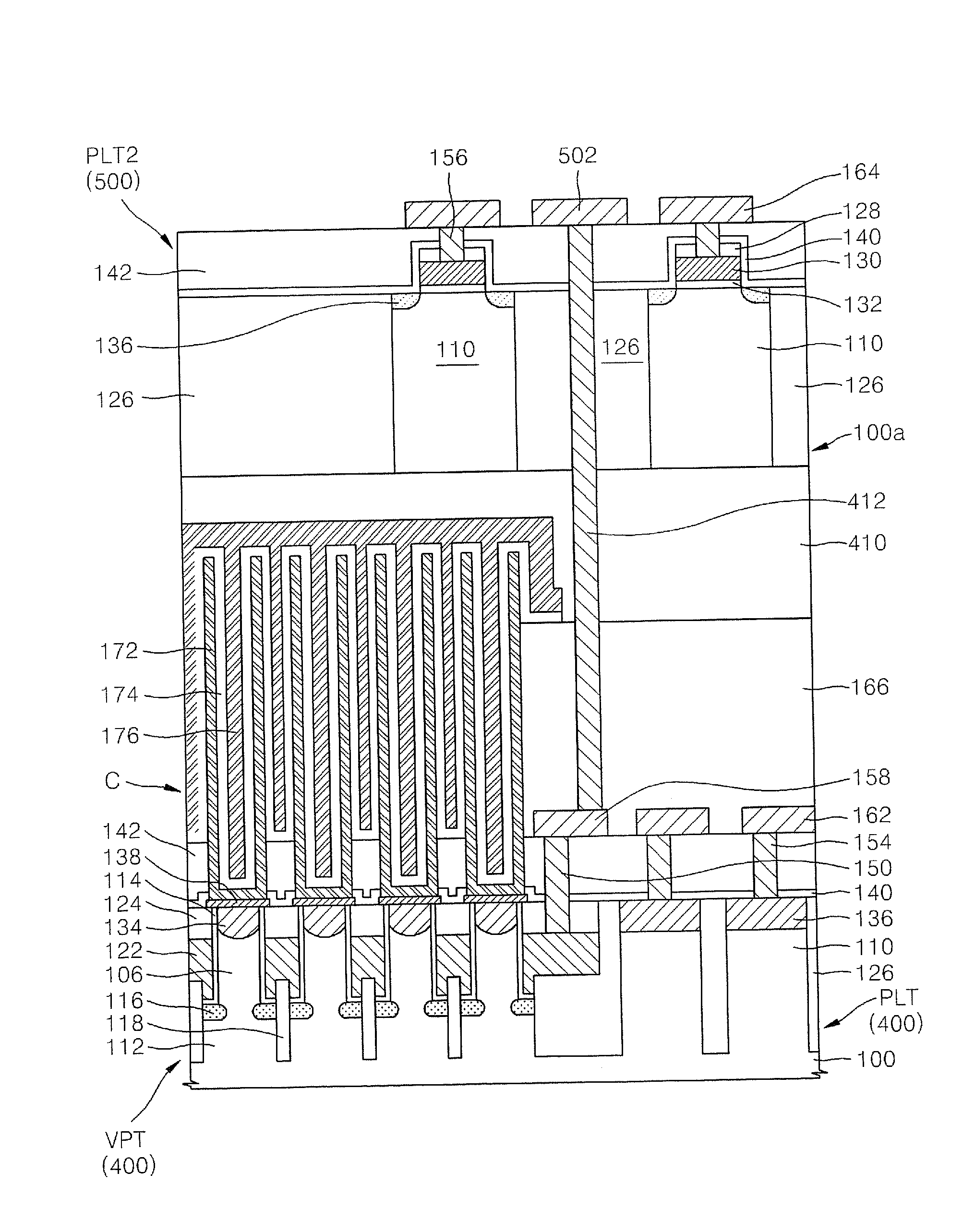
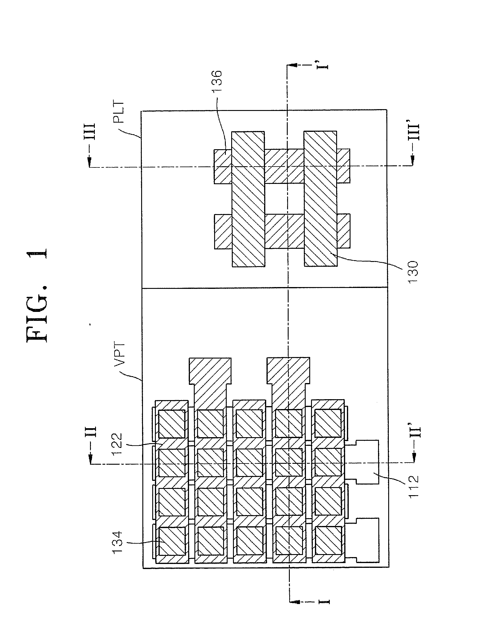
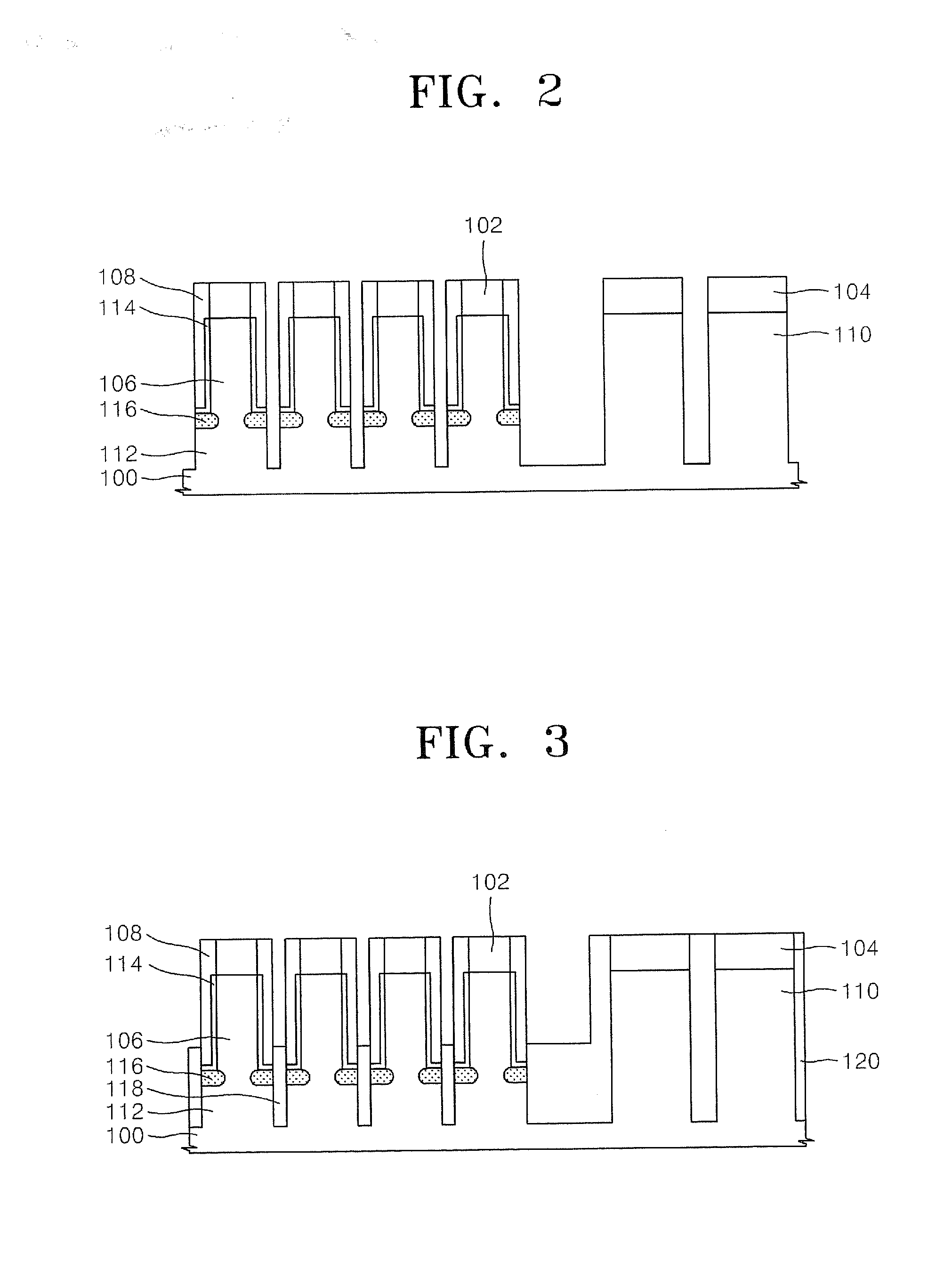
[0039]The present invention will now be described more fully with reference to the accompanying drawings, in which exemplary embodiments of the invention are shown. The invention may, however, be embodied in many different forms and should not be construed as being limited to the embodiments set forth herein; rather, these embodiments are provided so that this disclosure will be thorough and complete, and will fully convey the concept of the invention to those skilled in the art. In the drawings, the dimensions of substrates, layers, regions or patterns are exaggerated for clarity. It will also be understood that when a layer, a region, a pad or a pattern is referred to as being “on” another substrate, layer region or pad, it can be directly on the other layer, region, pad or pattern, or intervening layers, regions, pads or patterns may also be present.

[0040]Also, though terms like a first and a second are used to describe various members, components, regions, layers, and / or portion...


PUM


Abstract

An integrated circuit semiconductor device includes a first transistor formed at a lower substrate and configured with at least one of a vertical transistor and a planar transistor. A bonding insulation layer is formed on the first transistor, and an upper substrate is bonded on the bonding insulation layer. A second transistor configured with at least one of a vertical transistor and a planar transistor is formed at the upper substrate. The first transistor and the second transistor are connected by an interconnection layer.

Description

REFERENCE TO PRIORITY APPLICATION[0001]This application claims priority from Korean Patent Application No. 10-2007-0107417, filed Oct. 24, 2007, the disclosure of which is hereby incorporated herein by reference.FIELD OF THE INVENTION[0002]The present invention relates to integrated circuit devices and methods of forming same and, more particularly, to vertically integrated circuits and methods of forming same.BACKGROUND OF THE INVENTION[0003]An increase in integration density of an integrated circuit semiconductor device (semiconductor chip) is drastically decreasing the design rule in order to integrate more transistors in a limited substrate area. As a result, an area and length of a transistor in a cell area (hereinafter, referred to as a cell array transistor) of the integrated semiconductor device such as a dynamic random access memory (DRAM) device are greatly decreasing.[0004]The decrease in the design rule of the integrated circuit semiconductor device results in a short-ch...

Claims


Application Information

Patent Timeline
Patent Type & Authority Applications(United States)
IPC IPC(8): H01L27/108
CPCH01L21/8221H01L27/0688H01L27/10817H01L29/66666H01L27/10894H01L27/10897H01L27/10876H10B12/318H10B12/053H10B12/09H10B12/50H10B12/36H10B12/395H10B12/0383H10B12/056
Inventor YOON, JAE-MANOH, YONG-CHULKIM, HUI-JUNGCHUNG, HYUN-WOOKIM, KANG-UKPARK, DONG-GUNYANG, WOUN-SUCK
Owner SAMSUNG ELECTRONICS CO LTD
Why Eureka
Try Eureka