Chip stack package

Active Publication Date: 2009-04-30
SAMSUNG ELECTRONICS CO LTD
View PDF10 Cites 20 Cited by
  • Summary
  • Abstract
  • Description
  • Claims
  • Application Information

AI Technical Summary

Benefits of technology

[0008]The present invention provides a chip stack package having improved electrical characteristics.

Problems solved by technology

However, since the chips are connected to each other using the through via electrode in the chip stack package, the electrical characteristics of the chip stack package can deteriorate.

Method used


Image

  • Chip stack package
  • Chip stack package
  • Chip stack package

Examples


Embodiment Construction

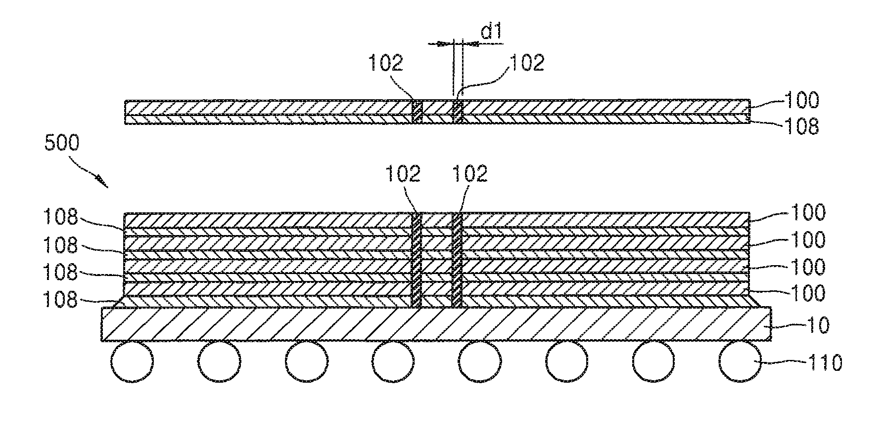
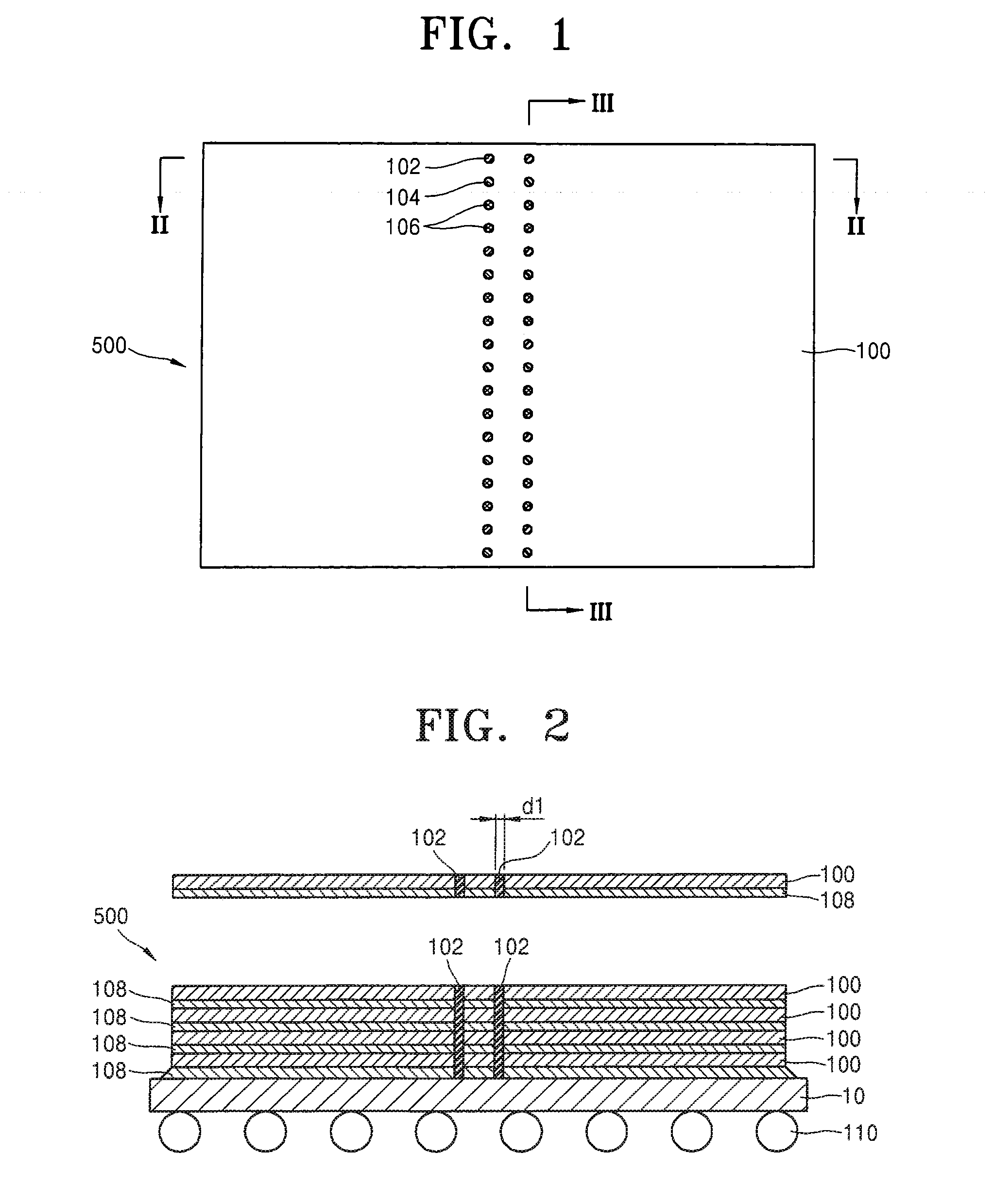
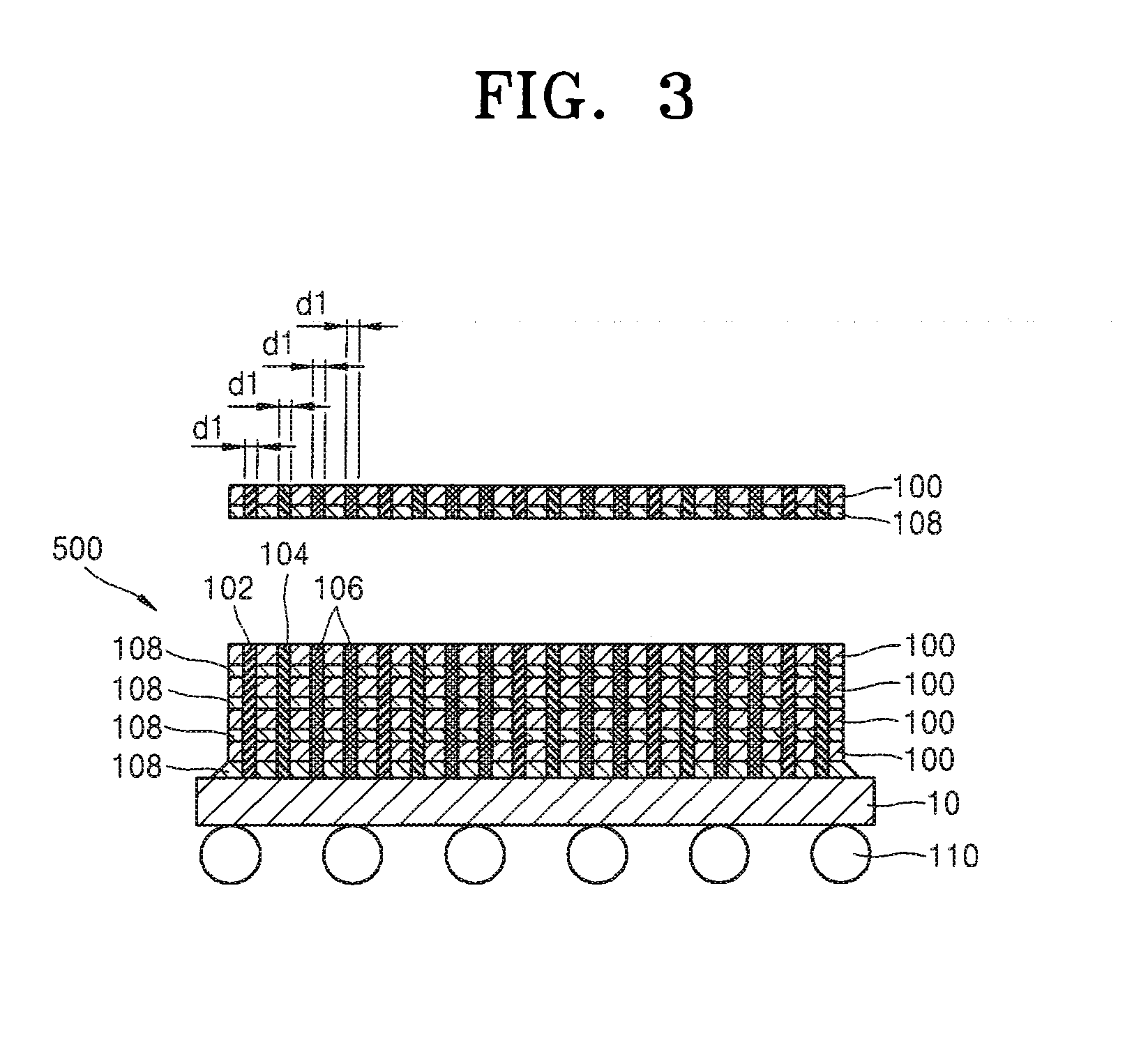
[0025]The present invention can be applied to a chip stack package including chips stacked at a wafer level or a chip level. In particular, the present invention can be applied to a chip stack package including chips stacked at a wafer level, i.e., a wafer stack package. In the wafer stack package, the thickness of each of the stacked chips can be reduced, thereby reducing the thickness of the wafer stack package.

[0026]In the chip stack package including the chips stacked at a wafer level and a chip level, a through via electrode may have three classifications: a power supply through via electrode, a ground through via electrode, and a signal transfer through via electrode. In addition, the chip stack package may be configured so that the power supply through via electrode, the ground through via electrode, and the signal transfer through via electrode have relatively different diameters, and may be formed of relatively different materials according to their electrical characteristi...


PUM


Abstract

A chip stack package includes a plurality of chips that are stacked by using adhesive layers as intermediary media, and a through via electrode formed through the chips to electrically couple the chips. The through via electrode is classified as a power supply through via electrode, a ground through via electrode, or a signal transfer through via electrode. The power supply through via electrode and the ground through via electrode are formed of a first material such as copper, and the signal transfer through via electrode is formed of second material such as polycrystalline silicon doped with impurities. The signal transfer through via electrode may have a diametrically smaller cross section than that of each of the power supply through via electrode and the ground through via electrode regardless of their resistivities.

Description

CROSS-REFERENCE TO RELATED PATENT APPLICATION[0001]This application claims the benefit of Korean Patent Application No. 10-2007-0109698, filed on Oct. 30, 2007, in the Korean Intellectual Property Office, the disclosure of which is incorporated herein in its entirety by reference.BACKGROUND[0002]1. Field of the Invention[0003]The present invention relates to a chip stack package, and more particularly, to a chip stack package including chips that are stacked at a wafer level or a chip level.[0004]2. Description of the Related Art[0005]A recent trend of the semiconductor industry is to make inexpensive semiconductor products compact, thin, light, fast, multifunctional and highly-efficient, so as to have high reliability. To achieve this, a package technology has been used as one of the important technologies for designing such semiconductor products.[0006]For example, a chip stack package is a chip-sized package, and is configured by stacking chips at a wafer level or a chip level if...

Claims


Application Information

Patent Timeline
IPC IPC(8): H01L23/538
CPCH01L25/0657H01L2224/16145H01L2924/15311H01L2225/06541H01L2225/06513H01L2224/05573H01L2224/13025H01L2224/16146H01L2224/32145H01L2224/06155H01L24/06H01L24/05H01L24/16H01L23/12
Inventor KANG, SUN-WONBAEK, SEUNG-DUKLEE, JONG-JOO
Owner SAMSUNG ELECTRONICS CO LTD
Why Eureka
Try Eureka