
Organic semiconductor compound, organic thin film including same, and electronic device including the organic thin film

Inactive Publication Date: 2016-05-26
SAMSUNG ELECTRONICS CO LTD
View PDF0 Cites 1 Cited by
  • Summary
  • Abstract
  • Description
  • Claims
  • Application Information

AI Technical Summary

Benefits of technology

Example embodiments describe a new compound that has high charge mobility due to its compact structure. It also provides a thin film that improves electrical characteristics of electronic devices.

Problems solved by technology

However, the polymer organic material has relatively low charge mobility but a relatively high blocking leakage current.
On the other hand, the relatively low molecular organic material such as pentacene, etc. is reported to have relatively high charge mobility of greater than or equal to about 3.2 to about 5.0 cm2 / Vs, but needs expensive vacuum deposition equipment to form a thin film, and thus may not be appropriate in terms of processibility and formation of a large area.

Method used

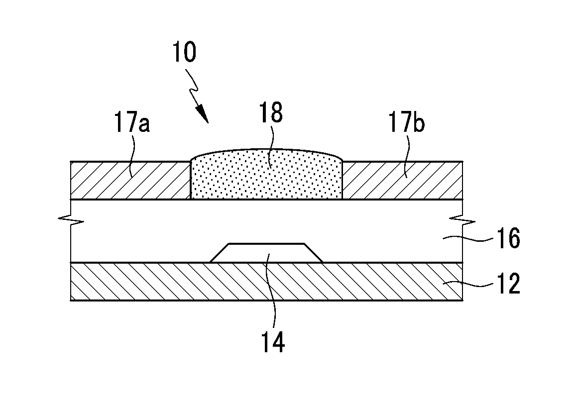
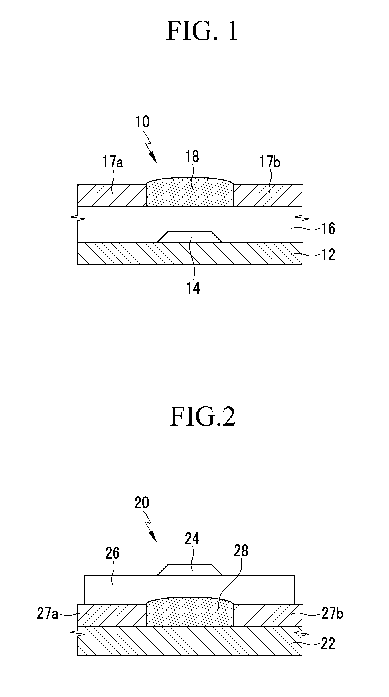
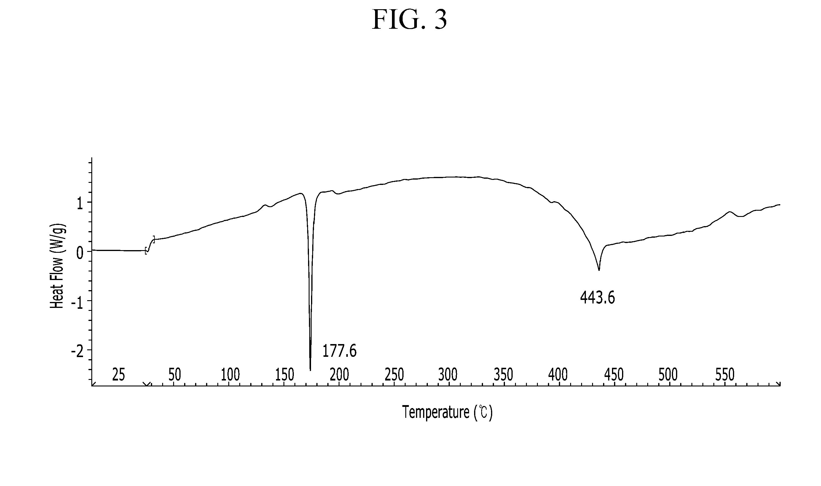

Image

  • Organic semiconductor compound, organic thin film including same, and electronic device including the organic thin film
  • Organic semiconductor compound, organic thin film including same, and electronic device including the organic thin film
  • Organic semiconductor compound, organic thin film including same, and electronic device including the organic thin film

Examples


example 1

Synthesis of Organic Semiconductor Compound (1)

[0091]The organic semiconductor compound (1) is synthesized according to Reaction Scheme 1 by using a method described in Synlett, 2006, 7, 1021 and J. Heterocycl. Chem. 2007, 44, 161.

[0092]1H-NMR (CDI3, 300 MHz) d 12.18 (s, 2H), 8.36 (d, 2H), 8.27 (d, 2H), 8.22 (d, 2H), 7.67 (d, 2H), 7.44 (d, 2H), 7.26 (d, 2H).

[0093]13C-NMR (CDCl3, 75 MHz) d 141.3, 138.5, 123.3, 121.4, 120.0, 119.8, 118.8, 115.3, 111.1, 103.0.

example 2

Synthesis of Organic Semiconductor Compound (2)

[0094]The organic semiconductor compound (2) is synthesized according to Reaction Scheme 2. First, the organic semiconductor compound (1) of Example 1 (3 g, 9.8 mmol) is dissolved in 200 mL of dimethyl sulfoxide (DMSO), KOH (2.3 g, 39.2 mmol) and 1-iodohexane (7.4 mL, 48.9 mmol) are added thereto, and the mixture is stirred at 75° C. for 2 hours. When the reaction is terminated, the resultant is purified through column chromatography.

[0095]1H-NMR (CDI3, 300 MHz) d 8.37 (d, 2H), 8.31 (d, 2H), 8.19 (d, 2H), 7.58 (d, 2H), 7.52 (dd, 2H), 7.34 (t, 2H), 4.83 (t, 4H), 2.14 (m, 4H), 1.58 (m, 4H), 1.44 (m, 8H), 0.93 (t, 6H)

[0096]13C-NMR (CDCl3, 75 MHz) d 141.2, 136.5, 125.0, 123.1, 121.7, 119.8, 119.7, 118.9, 118.5, 114.3, 109.5, 46.8, 31.8, 30.5, 27.0, 22.8, 14.2

example 3

Synthesis of Organic Semiconductor Compound (3)

[0097]The organic semiconductor compound (3) is synthesized according to Reaction Scheme 3. First, the organic semiconductor compound (1) of Example 1 (3 g, 9.8 mmol) is dissolved in 200 mL of dimethyl sulfoxide (DMSO), KOH (2.3 g, 39.2 mmol) and 1-iodooctane (9.0 mL, 48.9 mmol) are added thereto, and the mixture is stirred at 75° C. for 2 hours. When the reaction is terminated, the resultant is purified through column chromatography.

[0098]1H-NMR (CDI3, 300 MHz) d 8.39 (d, 2H), 8.31 (d, 2H), 8.19 (d, 2H), 7.58 (d, 2H), 7.52 (t, 2H), 7.50 (t, 2H), 4.83 (t, 4H), 2.15 (m, 4H), 1.58 (m, 4H), 1.43 (m, 4H), 1.34 (m, 12H), 0.98 (t, 6H)

[0099]13C-NMR (CDCl3, 75 MHz) d 141.3, 136.5, 125.1, 123.2, 121.8, 119.8, 119.7, 118.9, 118.4, 114.3, 109.5, 46.8, 32.0, 30.3, 29.6, 29.4, 27.3, 22.8, 14.3


PUM


Abstract

An organic semiconductor compound represented by Chemical Formula 1 is highly fused due to fusion of greater than or equal to 4 rings, and has smooth intermolecular charge transfer due to relatively high planarity.

Description

CROSS REFERENCE TO RELATED APPLICATIONS[0001]This application claims priority to and the benefit of Korean Patent Application No. 10-2014-0166827 filed in the Korean Intellectual Property Office on Nov. 26, 2014, the entire contents of which are incorporated herein by reference.BACKGROUND[0002]1. Field[0003]Example embodiments relate to an organic semiconductor compound, an organic thin film including the same, and an electronic device including the organic thin film.[0004]2. Description of the Related Art[0005]In general, flat display devices, e.g., liquid crystal displays or organic electroluminescent displays, are provided with a variety of thin film transistors (TFTs) to drive the devices. The TFT may include a gate electrode, source / drain electrodes, and a semiconductor layer that may be activated in response to operation of the gate electrode. The semiconductor layer may include an organic semiconductor material that is controlled by a current between the source electrode and ...

Claims


Application Information

Patent Timeline
IPC IPC(8): H01L51/00C07D487/04
CPCH01L51/0072H01L51/0558C07D487/04Y02E10/549H10K85/6572H10K10/484H10K10/466
Inventor YANG, HYEYEONYUN, YOUNGJUNHAHM, SUK GYUPARK, JEONG ILCHUNG, JONG WONLEE, SANG YOON
Owner SAMSUNG ELECTRONICS CO LTD
Learn More