
Semiconductor device

Active Publication Date: 2015-10-01
SK HYNIX INC
View PDF2 Cites 1 Cited by
  • Summary
  • Abstract
  • Description
  • Claims
  • Application Information

AI Technical Summary

Benefits of technology

The present invention relates to a semiconductor device with improved electrical characteristics for high voltage applications. It provides a semiconductor device with a high-voltage supply circuit, a discharge circuit, and an auxiliary-voltage supply circuit. Additionally, a transfer circuit is provided to transfer an input voltage in response to the high voltage and the auxiliary voltage. In another embodiment, a memory block is included with memory cells and a transfer circuit for transferring operation voltages of global lines to local lines in response to the high voltage and the auxiliary voltage. These features enable improved performance and reliability of the semiconductor device for high voltage applications.

Problems solved by technology

However, there are breakdown characteristics as a result of internal high voltage applications which increase as size of the semiconductor device becomes smaller.
Worsening of the breakdown characteristics degrades the overall electrical characteristics of the semiconductor device.

Method used


Image

  • Semiconductor device
  • Semiconductor device
  • Semiconductor device

Examples


Embodiment Construction

[0022]Throughout the specification, it will be understood that when an element is referred to as being “connected” or “coupled” to another element, it can be directly connected or coupled to the other element or intervening elements may be present. Further, it will be further understood that the terms “comprises,”“comprising”“includes,” and / or “including,” when used herein, specify the presence of stated features, items, steps, operations, elements, and / or components, but do not preclude the presence or addition of one or more other features, items, steps, operations, elements, components, and / or groups thereof.

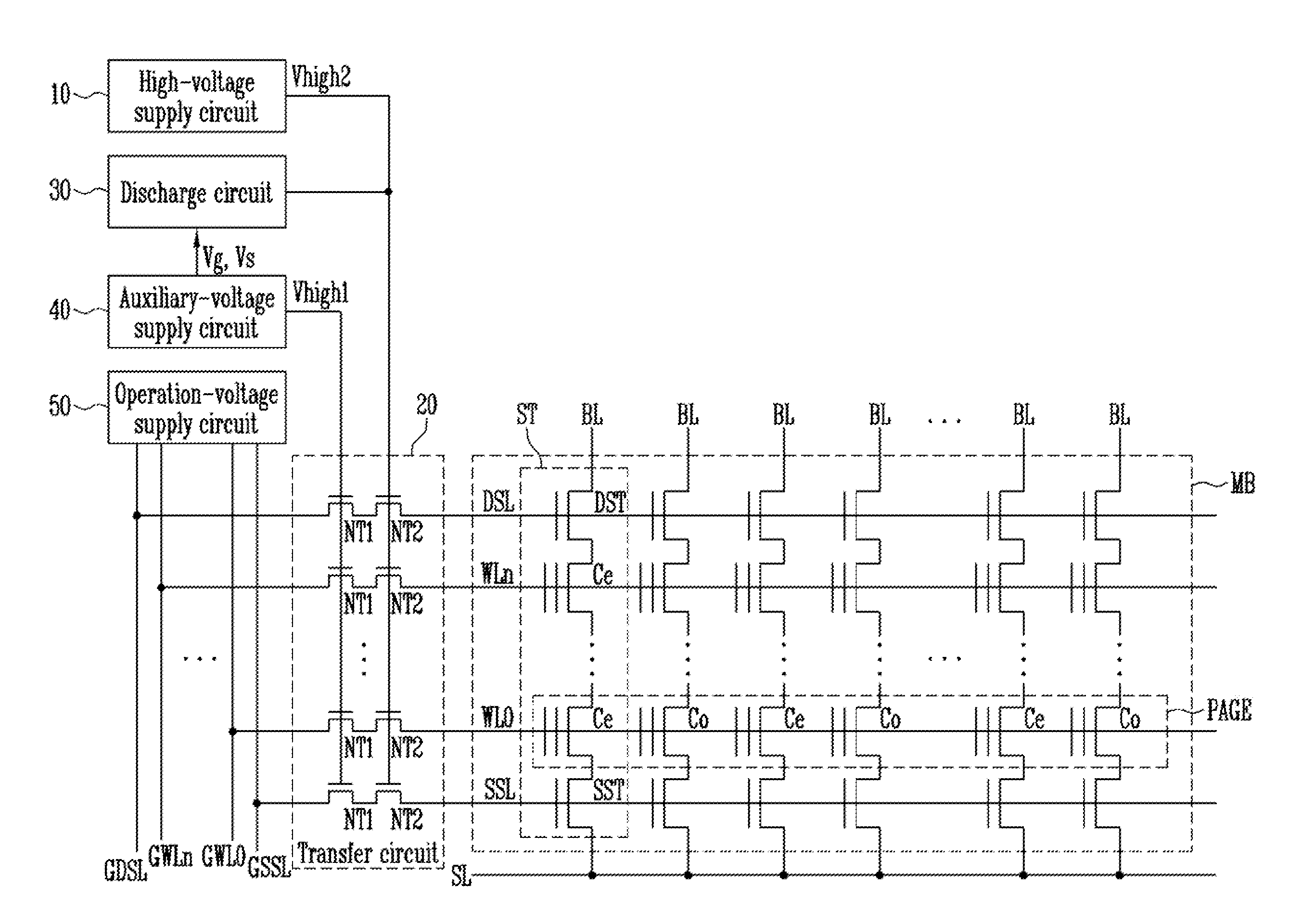
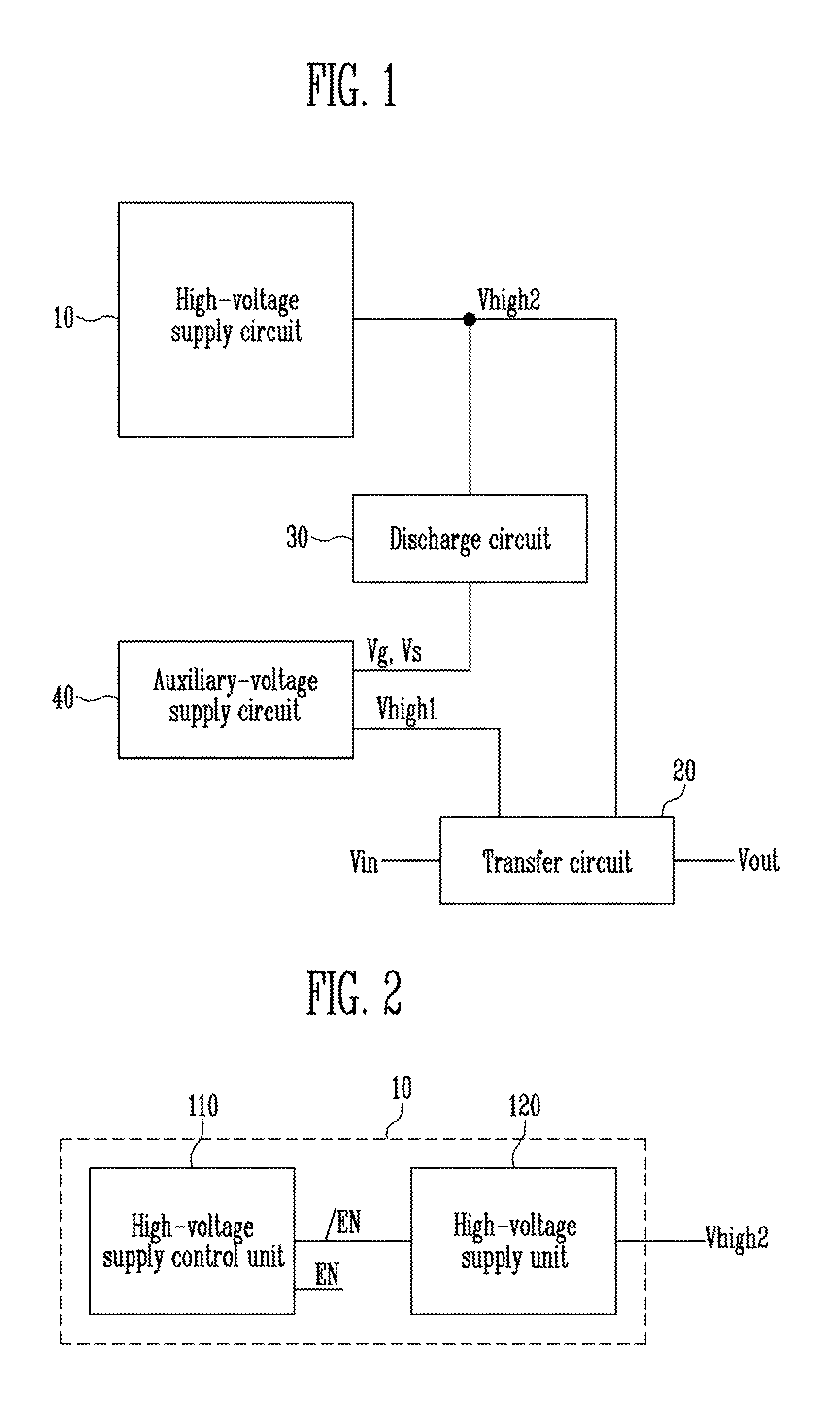
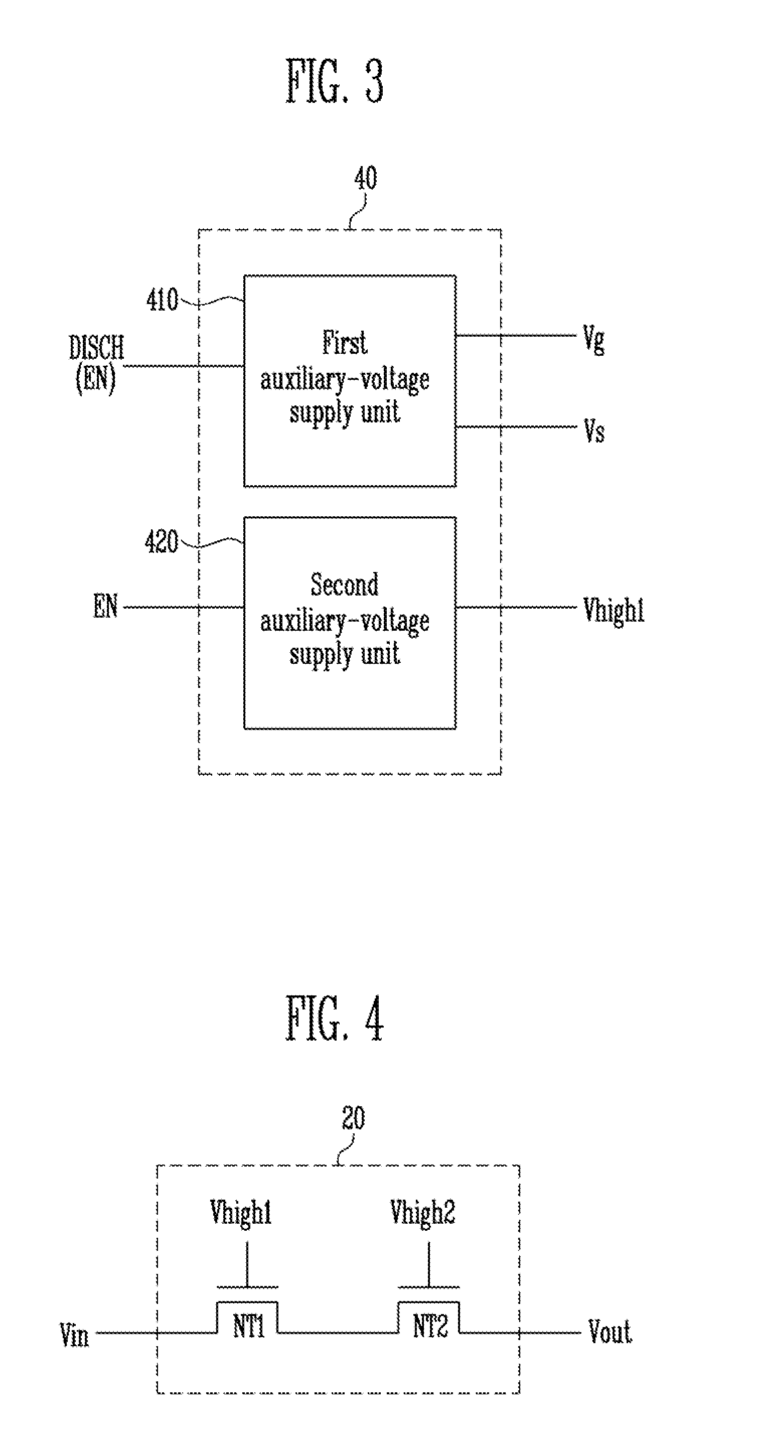
[0023]FIG. 1 is a block diagram illustrating a semiconductor device according to an embodiment. FIG. 2 is a block diagram illustrating a high-voltage supply circuit shown in FIG. 1. FIG. 3 is a block diagram illustrating an auxiliary-voltage supply circuit shown in FIG. 1. FIG. 4 is a circuit diagram illustrating a transfer circuit shown in FIG. 1. FIG. 5 is a circuit diagram...


PUM


Abstract

A semiconductor device, wherein the semiconductor device includes a high-voltage supply circuit suitable for supplying a high voltage; a discharge circuit suitable for discharging the high voltage; and an auxiliary-voltage supply circuit suitable for supplying a first auxiliary voltage, which varies according to an operation state of the high-voltage supply circuit, to a reference node of the discharge circuit.

Description

CROSS-REFERENCE TO RELATED APPLICATION[0001]The present application claims priority to Korean patent application number 10-2014-0038817, filed on Apr. 1, 2014, the entire disclosure of which is incorporated herein in its entirety by reference.BACKGROUND[0002]1. Field of Invention[0003]Various exemplary embodiments of the present invention relate to a semiconductor device, and more specifically to a semiconductor device using a high voltage.[0004]2. Description of Related Art[0005]Although the external voltage supplied to semiconductor device is generally low, a high internal voltage is still. To this end, the semiconductor device internally generates and uses a high voltage.[0006]However, there are breakdown characteristics as a result of internal high voltage applications which increase as size of the semiconductor device becomes smaller. Worsening of the breakdown characteristics degrades the overall electrical characteristics of the semiconductor device.SUMMARY[0007]Various exemp...

Claims


Application Information

Patent Timeline
IPC IPC(8): G05B11/01G11C16/30
CPCG11C16/30G05B11/01H02J9/061
Inventor LEE, YEONGHUN
Owner SK HYNIX INC
Learn More