Semiconductor device and method of fabricating the same

Active Publication Date: 2022-03-03
SAMSUNG ELECTRONICS CO LTD
View PDF0 Cites 0 Cited by
  • Summary
  • Abstract
  • Description
  • Claims
  • Application Information

AI Technical Summary

Benefits of technology

The present invention provides a semiconductor device that has better electrical properties and increased reliability. Additionally, the invention offers a method of making the semiconductor device that reduces manufacturing costs and time.

Problems solved by technology

The scale down of the MOSFETs may deteriorate operating characteristics of the semiconductor device.

Method used


Image

  • Semiconductor device and method of fabricating the same
  • Semiconductor device and method of fabricating the same
  • Semiconductor device and method of fabricating the same

Examples


Embodiment Construction

[0014]The following will now describe a semiconductor device and a method of fabricating the same according to some embodiments of the present inventive concepts in conjunction with the accompanying drawings.

[0015]Herein, when one value is described as being about equal to another value, e.g. “a width may be from about 0.1 mm to about 1 mm”, it is to be understood that the values are equal to each other to within a measurement error, or if measurably unequal, are close enough in value to be functionally equal to each other as would be understood by a person haying ordinary skill in the art.

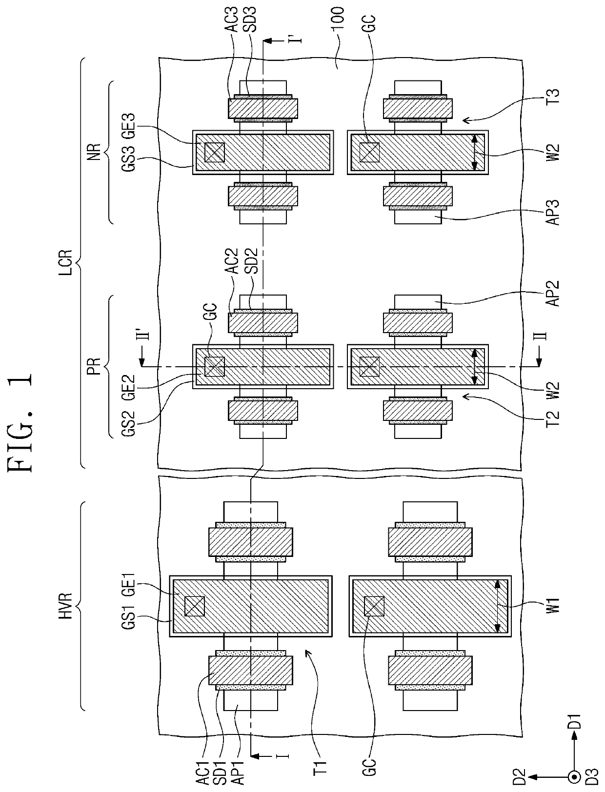
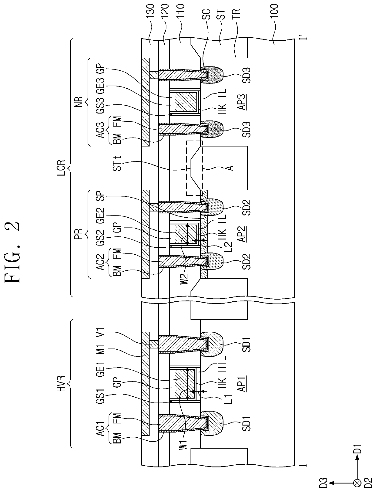
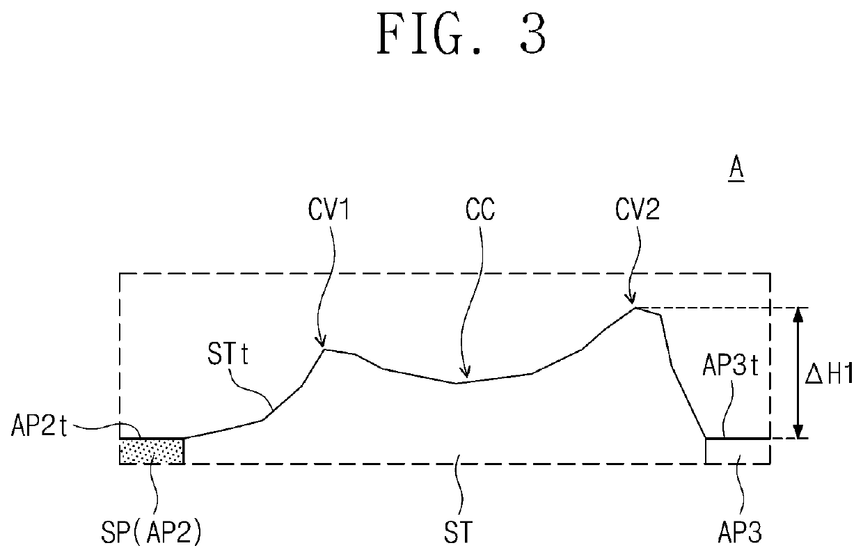
[0016]FIG. 1 is a plan view of a semiconductor device according to some embodiments of the present inventive concepts. FIGS. 2 and 4 are cross-sectional views taken along lines I-I′ and II-II′ of FIG. 1, of a semiconductor device according to some embodiments of the present inventive concepts. FIG. 3 is an enlarged view of section A of FIG. 2, of a semiconductor device according to some embodiment...


PUM


Abstract

A semiconductor device includes a substrate that includes peripheral and logic cell regions, a device isolation layer that defines a first active pattern on the peripheral region and second and third active patterns on the logic cell region, and first to third transistors on the first to third active patterns. Each of the first to third transistors includes a gate electrode, a gate spacer, a source pattern and a drain pattern. The second active pattern includes a semiconductor pattern that overlaps the gate electrode. At least a portion of a top surface of the device isolation layer is higher than a top surface of the second and third active patterns. A profile of the top surface of the device isolation layer includes two or more convex portions between the second and third active patterns.

Description

CROSS-REFERENCE TO RELATED APPLICATION[0001]This U.S. non-provisional application claims priority under 35 U.S.C § 119 from Korean Patent Application No. 10-2020-0112003, filed on Sep. 3, 2020 in the Korean Intellectual Property Office, the contents of which are herein incorporated by reference in their entirety.TECHNICAL FIELD[0002]Embodiments of the present inventive concepts are directed to a semiconductor device and a method of fabricating the same, and more particularly, to a semiconductor device that includes a field effect transistor and a method of fabricating the same.DISCUSSION OF THE RELATED ART[0003]A semiconductor device includes an integrated circuit that includes metal oxide semiconductor field effect transistors (MOSFETs). As sizes and design rules of semiconductor devices have gradually decreased, sizes of the MOSFETs have also been increasingly scaled down. The scale down of the MOSFETs may deteriorate operating characteristics of the semiconductor device. Accordin...

Claims


Application Information

Patent Timeline
IPC IPC(8): H01L27/088H01L29/06H01L27/108H01L29/423H01L21/02
CPCH01L27/088H01L29/0649H01L21/02532H01L29/42364H01L27/10894H01L21/02639H01L27/0922H01L21/823462H01L21/823807H01L21/823481H01L21/823878H01L29/42376H01L29/165H01L29/7848H01L29/1054H01L29/66651H01L29/41766H01L29/66636H01L29/66545H01L21/823468H01L21/823456H10B12/09
Inventor WOO, JONG SUNG
Owner SAMSUNG ELECTRONICS CO LTD
Why Eureka
Try Eureka