
Resistance change memory device

a memory device and resistance change technology, applied in the direction of information storage, static storage, digital storage, etc., can solve the problems of data retention on the high resistance state side of the reset state easily shifting to the reset state side,

Active Publication Date: 2009-04-30
KIOXIA CORP
View PDF7 Cites 47 Cited by
  • Summary
  • Abstract
  • Description
  • Claims
  • Application Information

AI Technical Summary

Benefits of technology

The present invention provides a resistance change memory device that can store multi-level data with at least three resistance values in a non-volatile manner. The device has memory cells that can be reset at the lowest resistance value and have resistance values selectively set for storing data. The resistance gaps between the different resistance values are set to satisfy a specific relationship to ensure the stability of the highest resistance value. This invention allows for the storage of more data in a smaller space and improves the reliability and stability of the memory device.

Problems solved by technology

For example, a high resistance state is defined as a reset state (i.e., thermally stabilized state) while a low resistance state is defined as a set state, and it becomes problematic that the set state easily shifts to the reset state side.
For example, in a PCRAM, the data retention on the high resistance state side usually becomes problematic.

Method used


Image

  • Resistance change memory device
  • Resistance change memory device
  • Resistance change memory device

Examples


Embodiment Construction

[0045]Illustrative embodiments of this invention will be explained with reference to the accompanying drawings below.

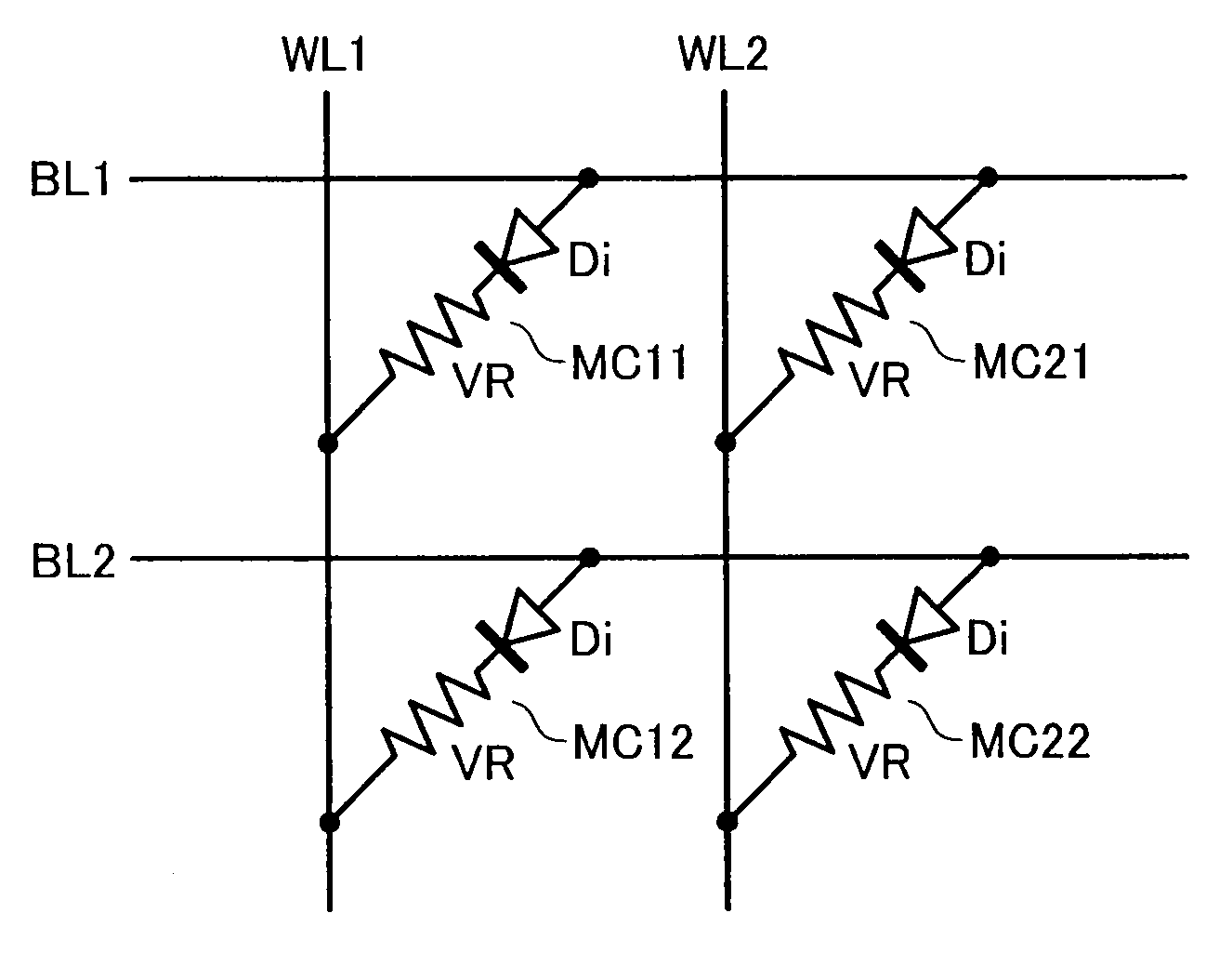
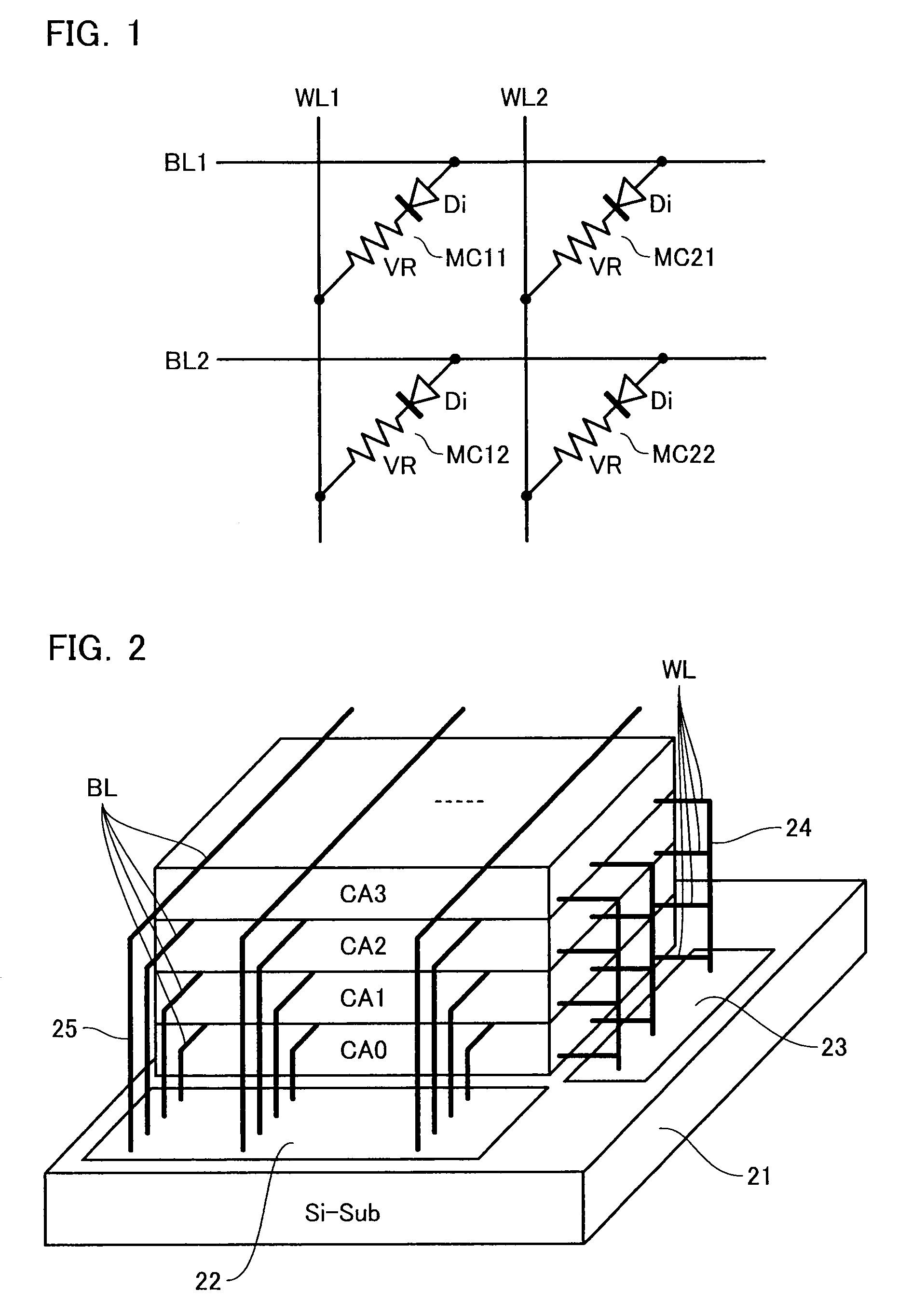
[0046]FIG. 1 shows an equivalent circuit of a cell array of a resistance change memory (ReRAM) in accordance with an embodiment. Word lines WLi (WL1, WL2, . . . ) and bit lines BLj (BL1, BL2, . . . ) are formed to cross each other, and memory cells MCij (MC11, MC12, . . . , MC21, MC22, . . . ) are disposed at the respective cross points.

[0047]Memory cell MC is formed of variable resistance element VR and diode Di connected in series. Variable resistance element VR stores a resistance value as data in a non-volatile manner, which is electrically or thermally settable. Although the detailed layout is not shown here, for example, diode Di and variable resistance element VR are stacked on word lines WL, and bit lines BL are disposed thereabove in perpendicular to the word lines.

[0048]To achieve a large capacitive ReRAM, as shown in FIG. 2, multiple cell arrays are stacked...


PUM


Abstract

A resistance change memory device including memory cells arranged, the memory cell having a stable state with a high resistance value and storing in a non-volatile manner such multi-level data that at least three resistance values, R0, R1 and R2 (R0<R1<R2) are selectively set, wherein resistance gaps ΔR1(=R1−R0) and ΔR2(=R2−R1) are set to satisfy the relationship of ΔR1>ΔR2.

Description

CROSS-REFERENCE TO RELATED APPLICATION[0001]This application is based on and claims the benefit of priority from the prior Japanese Patent Application No. 2007-269973, filed on Oct. 17, 2007, the entire contents of which are incorporated herein by reference.BACKGROUND OF THE INVENTION[0002]1. Field of the Invention[0003]This invention relates to a resistance change memory device, specifically relates to data retention thereof in case a multi-level data storage scheme is adapted.[0004]2. Description of the Related Art[0005]Recently, it is noticed that a resistance change memory succeeds to a conventional flash memory. The “resistance change memory” described here includes not only a narrow-sensed resistance change memory (ReRAM: Resistance RAM), which has a recoding layer formed of a transition metal oxide for storing a resistance value state in a non-volatile manner, but also a phase change memory (PCRAM: Phase Change RAM), which uses a crystalline state (i.e., conductor) and an amo...

Claims


Application Information

Patent Timeline
Patent Type & Authority Applications(United States)
IPC IPC(8): G11C11/00G11C11/416
CPCG11C11/56G11C11/5678G11C13/0004G11C13/0009G11C13/004G11C2213/72G11C13/0069G11C2211/5642G11C2213/11G11C2213/34G11C2213/56G11C13/0064
Inventor MAEJIMA, HIROSHIISOBE, KATSUAKITOKIWA, NAOYATAKASE, SATORUFUKUDA, YASUYUKIMUKAI, HIDEOINABA, TSUNEO
Owner KIOXIA CORP
Learn More