

Method for preparing a recessed transistor structure
- Summary
- Abstract
- Description
- Claims
- Application Information
AI Technical Summary
Benefits of technology
Problems solved by technology
Method used
Image

Examples
Embodiment Construction
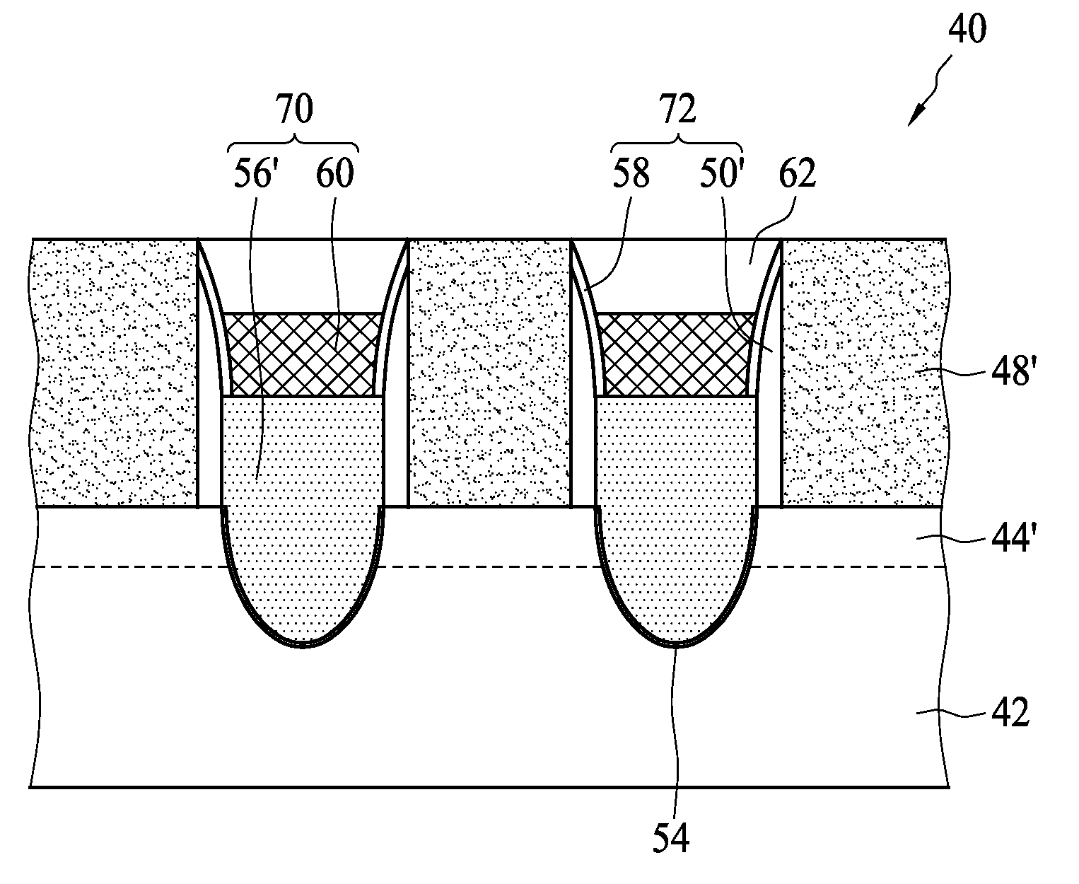
[0015]FIG. 7 to FIG. 17 illustrate a method for preparing a recessed transistor structure 40 according to the present invention. First, an implanting process is performed to form a doped layer 44 in an upper portion of a silicon substrate 42, and a photolithographic process is then performed to form a photoresist layer having a plurality of openings 46′ on the silicon substrate 42. Subsequently, a selective liquid-phase deposition process is performed to form an insulation layer 48 filling the openings 46′, as shown in FIG. 8. In particular, the selective liquid-phase deposition process selectively forms the insulation layer 48 only on the surface of the silicon substrate 42, not on the surface of the photoresist layer 46.
[0016]Referring to FIG. 9, after removing the photoresist layer 46, a thermal treating process is performed to solidify the insulation layer 48 such that the insulation layer 48 filling the openings 46′ forms a plurality of gate-isolation blocks 48′. Preferably, th...
PUM
 Abstract
Description
Claims
Application Information