Eureka AIR delivers breakthrough ideas for toughest innovation challenges, trusted by R&D personnel around the world.

Write driver circuit for phase-change memory, memory including the same, and associated methods

Inactive Publication Date: 2009-05-14
SAMSUNG ELECTRONICS CO LTD
View PDF11 Cites 16 Cited by
  • Summary
  • Abstract
  • Description
  • Claims
  • Application Information

AI Technical Summary

Benefits of technology

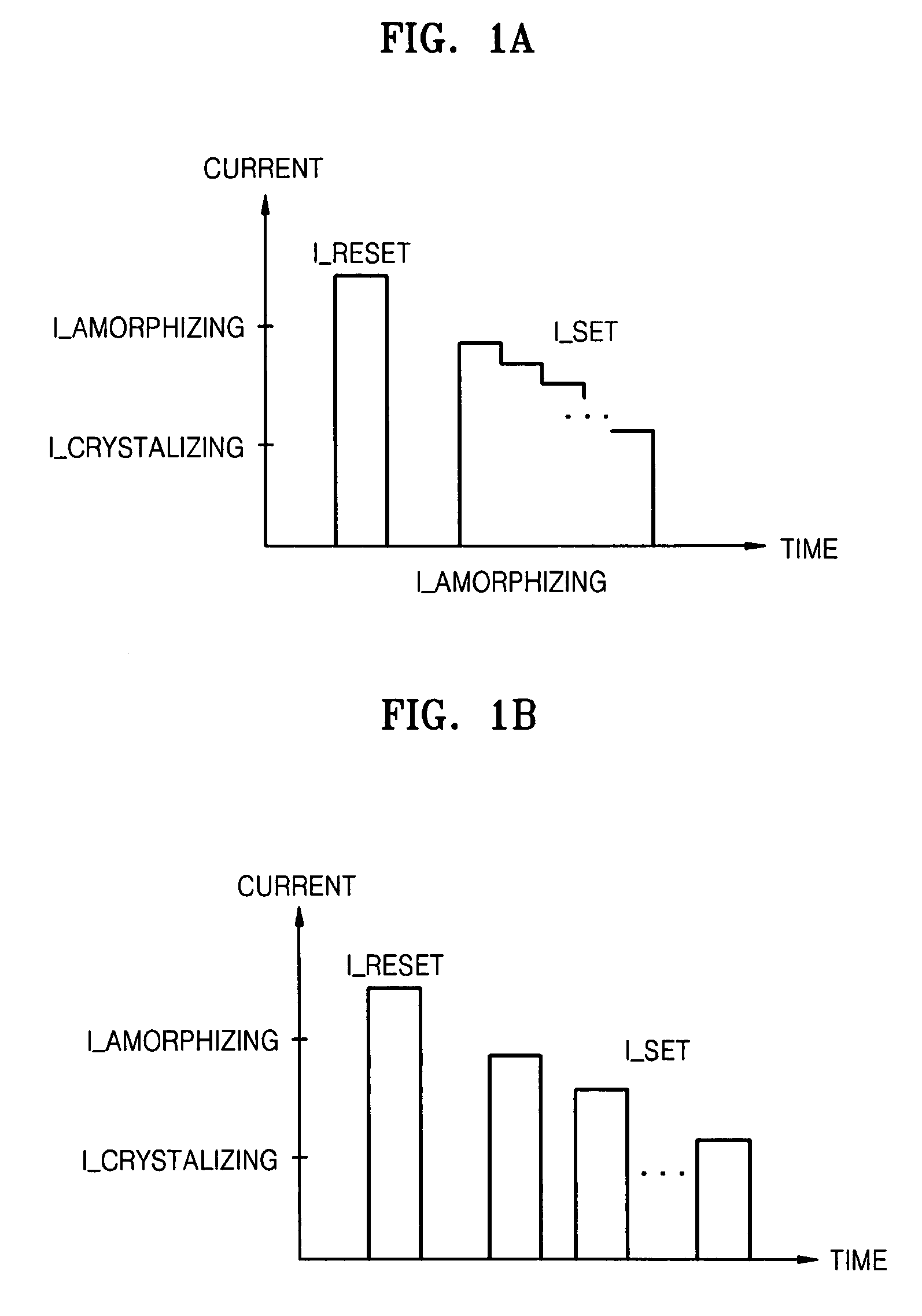
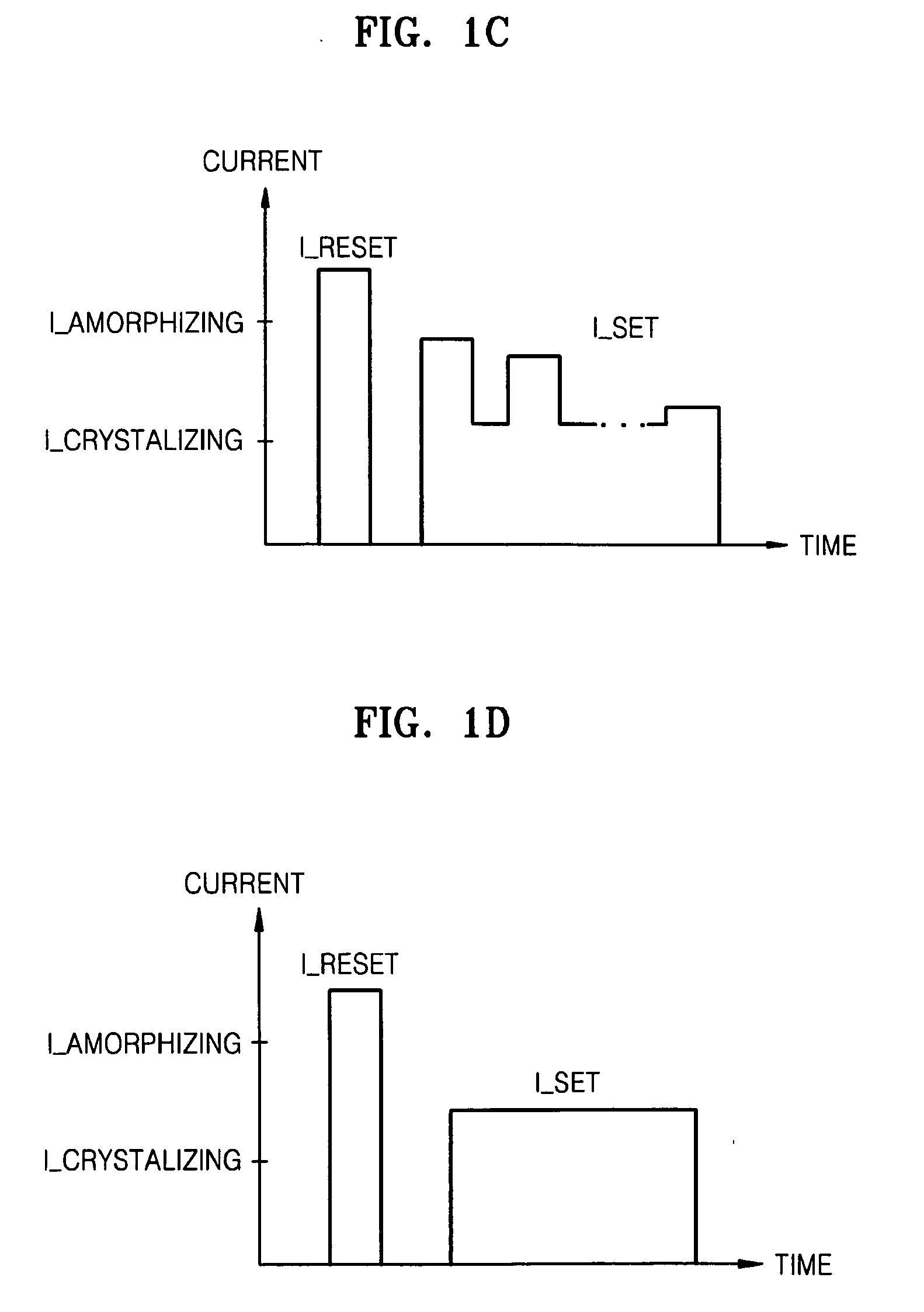
[0014]The reference current level may maintain the phase-change memory cells at a crystallizing temperature at which a phase-change material in the phase-change memory cells begin to crystallize, the crystallizing temperature being lower than a melting temperature of the phase-change material. The first SET state current level may change a phase-change memory cell requiring a highest current level for the SET state resistance among the phase-change memory cells, into the SET state resistance. The first SET state current level may not exceed a level of current that would heat the phase-change memory cells to their melting temperature.

Problems solved by technology

Further, there may be variations due to process margins in the manufacturing process.

Method used


Image

  • Write driver circuit for phase-change memory, memory including the same, and associated methods
  • Write driver circuit for phase-change memory, memory including the same, and associated methods
  • Write driver circuit for phase-change memory, memory including the same, and associated methods

Examples


Embodiment Construction

[0041]Korean Patent Application No. 10-2007-0115488, filed on Nov. 13, 2007, in the Korean Intellectual Property Office, and entitled: “Write Driver Circuit for Phase-Change Memory,” is incorporated by reference herein in its entirety.

[0042]Example embodiments will now be described more fully hereinafter with reference to the accompanying drawings; however, they may be embodied in different forms and should not be construed as limited to the embodiments set forth herein. Rather, these embodiments are provided so that this disclosure will be thorough and complete, and will fully convey the scope of the invention to those skilled in the art.

[0043]In the drawing figures, the dimensions of layers and regions may be exaggerated for clarity of illustration. It will be understood that when an element is referred to as being “between” two other elements, it can be the only element between the two other elements, or one or more intervening elements may also be present. Like reference numeral...


PUM


Abstract

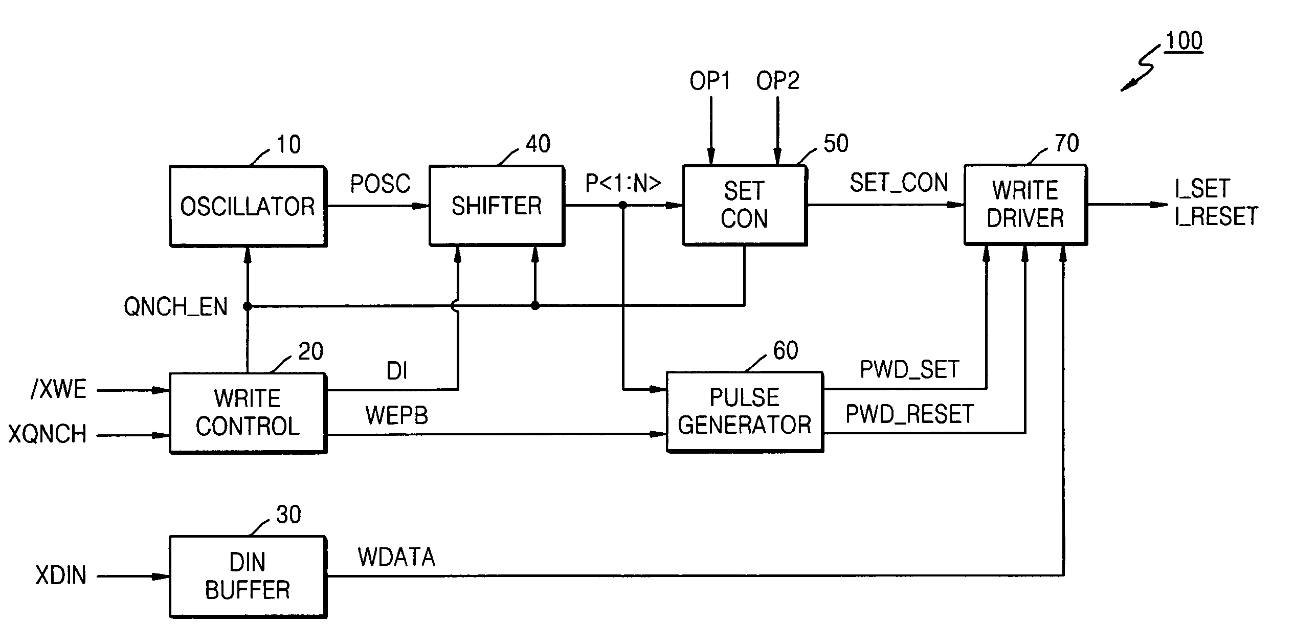
A write driver circuit for a memory that includes phase-change memory cells changeable between a RESET state resistance and a SET state resistance in response to an applied current pulse, the write driver circuit including a write current level adjusting unit configured to determine first to n-th SET state current levels in response to a SET state current level signal, where n is an integer greater than 1, and configured to determine a RESET state current level in response to a RESET state current level signal, and a write current output unit configured to generate one of a SET state current pulse and a RESET state current pulse corresponding to a SET state current level or a RESET state current level determined by the write current level adjusting unit.

Description

BACKGROUND[0001]1. Technical Field[0002]Embodiments relate to a semiconductor memory. More particularly, embodiments relate to a write driver circuit for a phase-change memory and a memory including the same.[0003]2. Description of the Related Art[0004]A Phase-change Random Access Memory (PRAM) is a nonvolatile memory device that stores data using a phase-change material, such as GST (Ge—Sb—Te), having a resistance that changes with a phase transition between amorphous and crystalline states. The phase transition may be controlled by controlling a temperature change and the time over which the phase change material is heated and cooled. The PRAM has characteristics of nonvolatility and low power consumption, as well as the advantages of a Dynamic Random Access Memory (DRAM).[0005]Either the crystalline state or the amorphous state of the phase-change material is selected by a level of current flowing through the phase-change material. High current supplied for a short period of time...

Claims


Application Information

Patent Timeline
IPC IPC(8): G11C11/00
CPCG11C8/08G11C13/0004G11C2013/0078G11C13/0038G11C13/0069G11C13/0028G11C13/02
Inventor CHO, BEAK-HYUNGKIM, KWANG-HOKIM, YOUNG-PIL
Owner SAMSUNG ELECTRONICS CO LTD
Why Eureka
Eureka Blog
Learn More