Display Device and Electronic Device

a technology of electronic devices and display devices, applied in static indicating devices, instruments, optics, etc., can solve the problem of limited device structure of optical sensors

Inactive Publication Date: 2009-05-21
SHARP KK
View PDF6 Cites 49 Cited by
  • Summary
  • Abstract
  • Description
  • Claims
  • Application Information

AI Technical Summary

Benefits of technology

[0031]In the display apparatus of the present invention, since a color filter for an optical sensor is provided on the optical sensor located in the display apparatus, the optical sensor is unaffected by ultraviolet rays or near infrared rays, and thus a change in illuminance of visible rays that affects the visibility can be detected precisely.

Problems solved by technology

On the other hand, if a display apparatus includes TFTs having the above structure in the display region, and an optical sensor for detecting the brightness of ambient light is formed monolithically in the peripheral region with an attempt to minimize an increase in the manufacturing process, the device structure of the optical sensor will have to be limited.

Method used


Image

  • Display Device and Electronic Device
  • Display Device and Electronic Device
  • Display Device and Electronic Device

Examples


embodiment 1

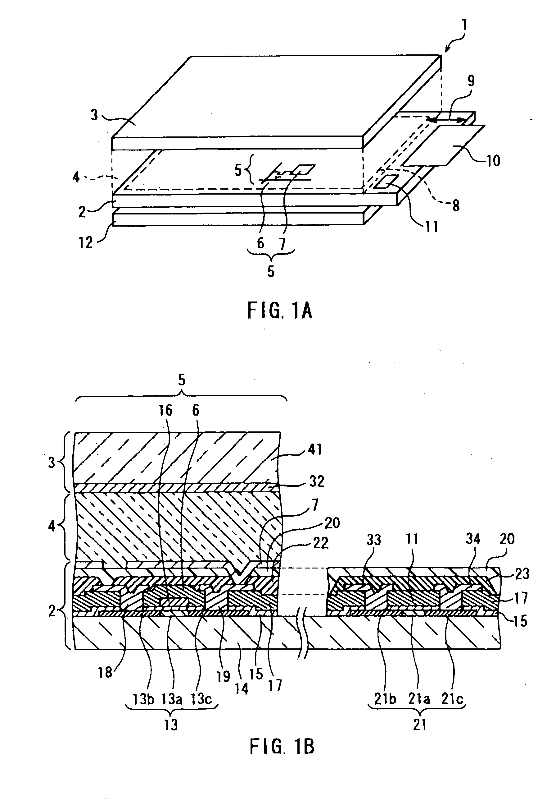
[0046]Hereinafter, a brief explanation of a display apparatus of Embodiment 1 of the present invention will be given by taking a liquid crystal display apparatus as an example with reference to the drawings.

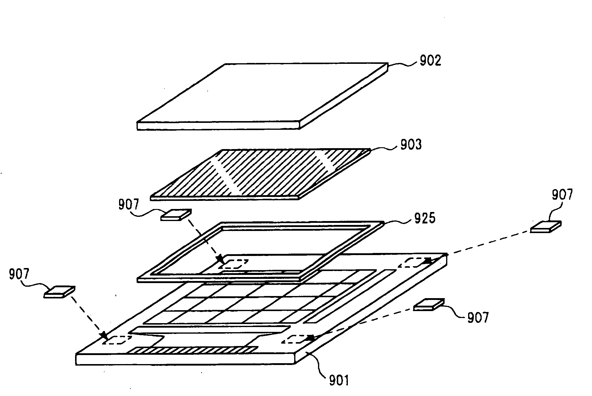
[0047]FIG. 1A is an entire configuration diagram of a display apparatus 1 of the present invention. The display apparatus 1 includes an active matrix substrate 2 on which a large number of pixels 5 are arranged in a matrix and a counter substrate 3 located opposite to the active matrix substrate 2. Moreover, the display apparatus 1 includes a display region (pixel array region) 8 in which the pixels 5 are arranged and a peripheral region 9 located close to the display region 8. The counter substrate 3 is provided so as to cover the display region 8 and to expose at least a part of the peripheral region 9 of the active matrix substrate 2.

[0048]The active matrix substrate 2 and the counter substrate 3 are bonded together with a frame-shaped sealing member (not shown) provided along...

embodiment 2

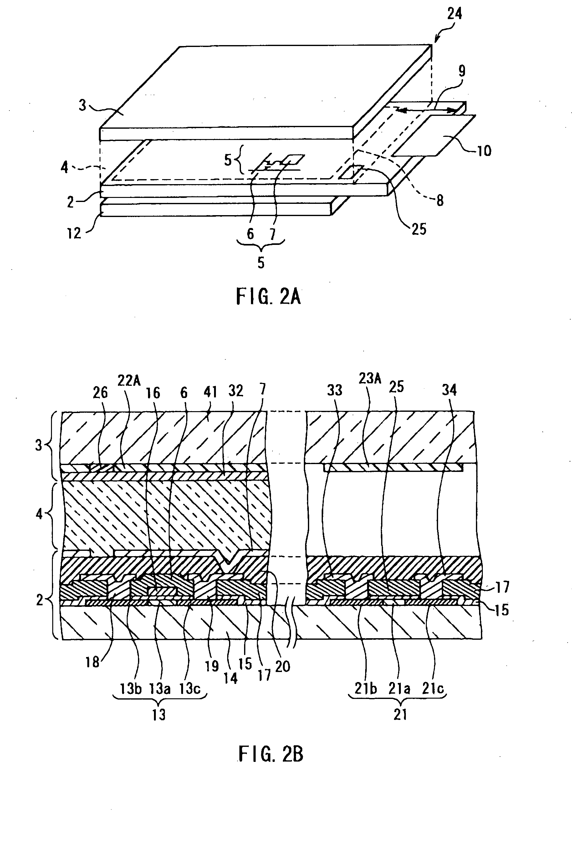
[0084]Embodiment 2 of the present invention describes a modified example of the display apparatus 1 as described in Embodiment 1. For convenience, the same components as those of the display apparatus 1 of Embodiment 1 are denoted by the same reference numerals, and the explanation may not be repeated.

[0085]FIG. 2A is an entire configuration diagram of a display apparatus 24 according to Embodiment 2 of the present invention. The display apparatus 24 includes an active matrix substrate 2 on which a large number of pixels 5 are arranged in a matrix and a counter substrate 3 located opposite to the active matrix substrate 2. Moreover, the display apparatus 24 includes a display region 8 in which the pixels 5 are arranged and a peripheral region 9 located close to the display region 8. The counter substrate 3 is provided so as to cover the display region 8 and to expose at least a part of the peripheral region 9 of the active matrix substrate 2.

[0086]The active matrix substrate 2 and t...

embodiment 3

[0097]Embodiment 3 of the present invention describes a modified example of the display apparatus 1 as described in Embodiment 1. For convenience, the same components as those of the display apparatus 1 of Embodiment 1 are denoted by the same reference numerals, and the explanation may not be repeated.

[0098]FIG. 3 is an entire configuration diagram of a display apparatus 27 according to Embodiment 3 of the present invention. The display apparatus 27 differs from the display apparatus 1 of Embodiment 1 in that a plurality of optical sensors 11 (three sensors are shown in FIG. 3) are formed in a peripheral region 9 of an active matrix substrate 2. Moreover, color filters 23 with different colors (red, blue, and green in FIG. 3) are formed on the respective optical sensors 11.

[0099]With this configuration, the display apparatus 27 can obtain the brightness information (e.g., red light of morning glow or sunset glow) of ambient light for each color (wavelength), and also can detect a co...


PUM

PropertyMeasurementUnit
thicknessaaaaaaaaaa
thicknessaaaaaaaaaa
thicknessaaaaaaaaaa

Abstract

A display apparatus including an optical sensor in its peripheral region is intended to response to visible rays efficiently by preventing a malfunction due to the reaction of the optical sensor to near ultraviolet rays. For this purpose, a display apparatus that includes an active matrix substrate (2) having a pixel array region (8) in which a plurality of pixels are arranged on a base substrate (14) is configured as follows: an optical sensor (11) is provided in a peripheral region (9) located around the pixel array region (8); a color filter (22) for display is provided on the opposite side of TFTs (6) from the base substrate (14); and a color filter (23) for an optical sensor is provided on the opposite side of the optical sensor (11) from the base substrate (14).

Description

TECHNICAL FIELD[0001]The present invention relates to a display apparatus such as a liquid crystal display apparatus or an electronic luminescent (EL) display apparatus. The present invention also relates to an electronic device including the display apparatus.BACKGROUND ART[0002]A flat panel type display apparatus, as typified by a liquid crystal display apparatus, has the characteristics of thinness, light weight, and low power consumption. Moreover, technical development is proceeding to improve the display performance such as coloring, high definition, and support for moving images. Therefore, the flat panel type display apparatus has currently been incorporated into electronic devices, e.g., a wide variety of information devices, TV devices, and amusement devices, such as a mobile telephone, personal digital assistants (PDA), a DVD player, a mobile game device, a notebook PC, a PC monitor, and a TV.[0003]In such a background, a technology for providing a display apparatus with ...

Claims


Application Information

Patent Timeline
Patent Type & Authority Applications(United States)
IPC IPC(8): G09G5/00G02F1/167
CPCG02F1/13318G02F1/167H01L31/02162H01L27/3269H01L27/322H10K59/38H10K59/13
Inventor IZUMI, YOSHIHIROUEHARA, KAZUHIRO
Owner SHARP KK
Why Eureka
Try Eureka