Apparatus and methods for precompiling program sequences for wafer processing

a program sequence and program technology, applied in the field of computer programs, can solve the problems of difficult and time-consuming modification of hardcode, high level determinism, and high complexity of semiconductor manufacturing techniques, and achieve the effects of minimizing problems, minimizing problems, and ensuring stability

Active Publication Date: 2009-05-21
NOVELLUS SYSTEMS
View PDF1 Cites 1 Cited by
  • Summary
  • Abstract
  • Description
  • Claims
  • Application Information

AI Technical Summary

Benefits of technology

[0007]In certain embodiments, operation of the hardware devices that are to be controlled by the program sequence and the translated instruction(s) may be simulated so as to verify that such operation is within a predetermined specification. The process for actually controlling the hardware device is then only executed after it has been determined that the simulation results specify that the simulated device operation is within this predetermined specification. Once execution of the program commences, the pre-compiled instructions that have been made accessible to selected lower-level controller(s) provide a very fast solution that has been pre-verified so as to instill confidence that the process control will reliably operate with minimal problems. In further aspects, the translated instructions and their associated interlock checks can also provide real time interlock checking between the various lower-level controllers and their underlying hardware devices to minimize problems associated with the operational interdependencies of the various hardware devices.

Problems solved by technology

Generally, the industry of semiconductor manufacturing involves highly complex techniques for fabricating integrating circuits from semiconductor materials that are layered and patterned onto a substrate, such as silicon, by various process systems.
However, a hardcoded solution does not allow a high level deterministic approach for verifying feedback prior to executing a next command, for example, and the hardcode can be difficult and time consuming to modify.

Method used


Image

  • Apparatus and methods for precompiling program sequences for wafer processing
  • Apparatus and methods for precompiling program sequences for wafer processing
  • Apparatus and methods for precompiling program sequences for wafer processing

Examples


Embodiment Construction

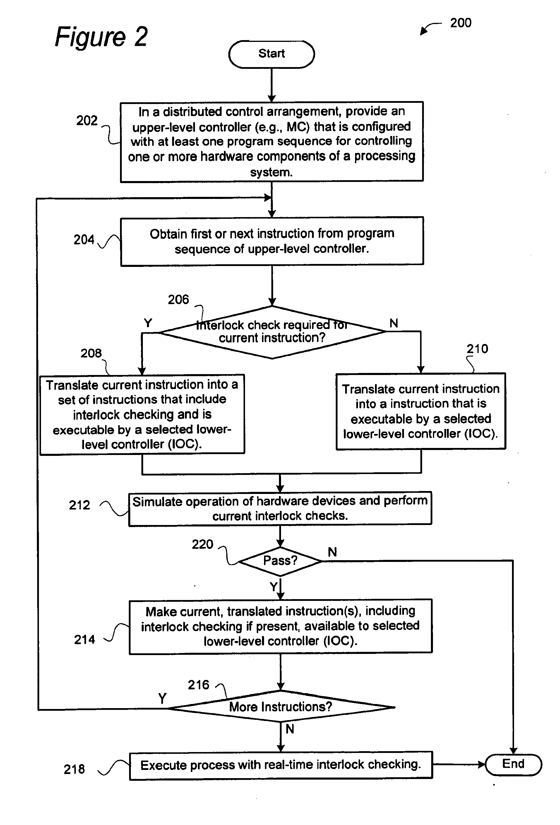
[0017]Reference will now be made in detail to a specific embodiment of the invention. An example of this embodiment is illustrated in the accompanying drawings. While the invention will be described in conjunction with this specific embodiment, it will be understood that it is not intended to limit the invention to one embodiment. On the contrary, it is intended to cover alternatives, modifications, and equivalents as may be included within the spirit and scope of the invention as defined by the appended claims. In the following description, numerous specific details are set forth in order to provide a thorough understanding of the present invention. The present invention may be practiced without some or all of these specific details. In other instances, well known procedure operations have not been described in detail in order not to unnecessarily obscure the present invention.

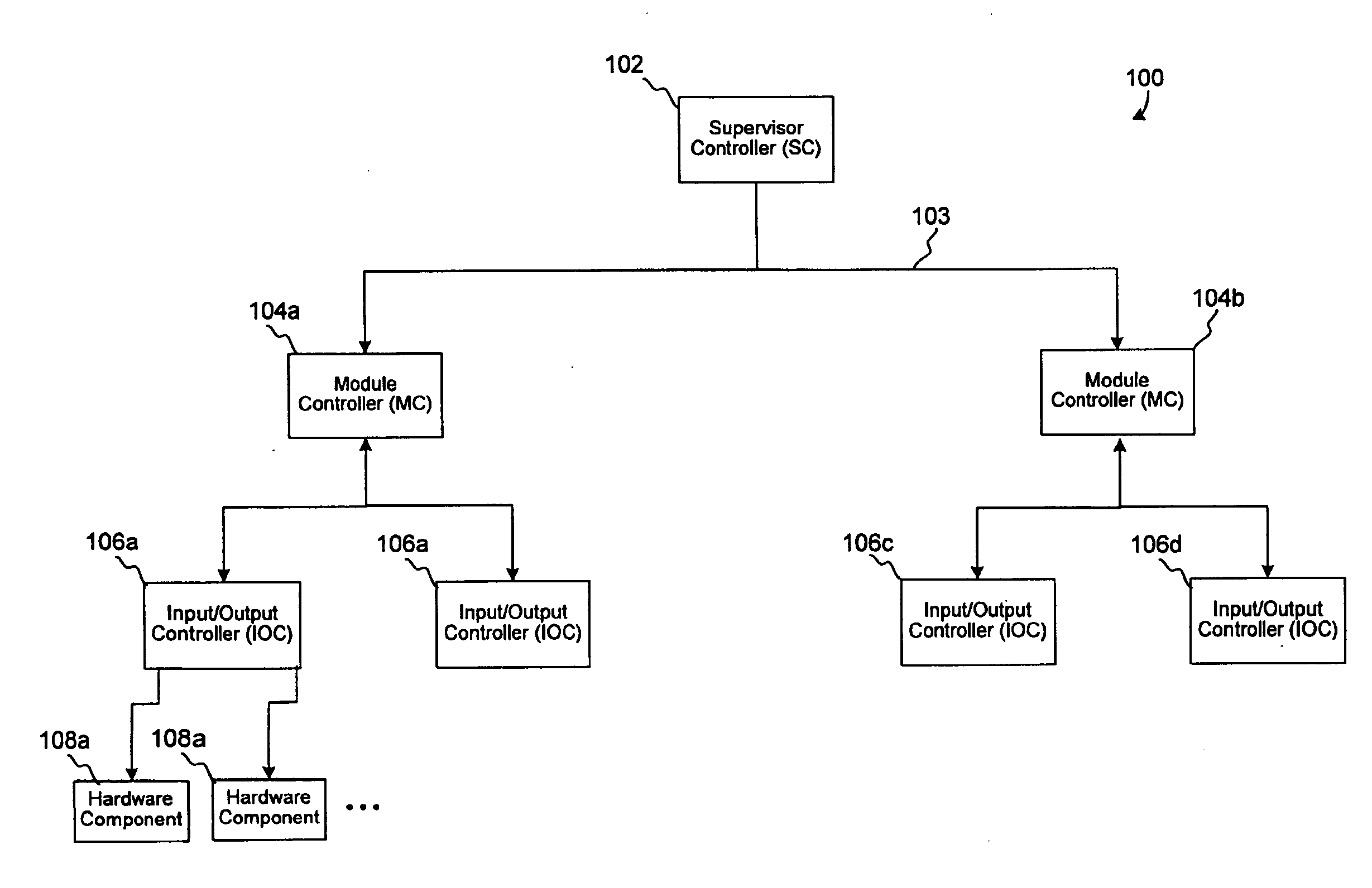
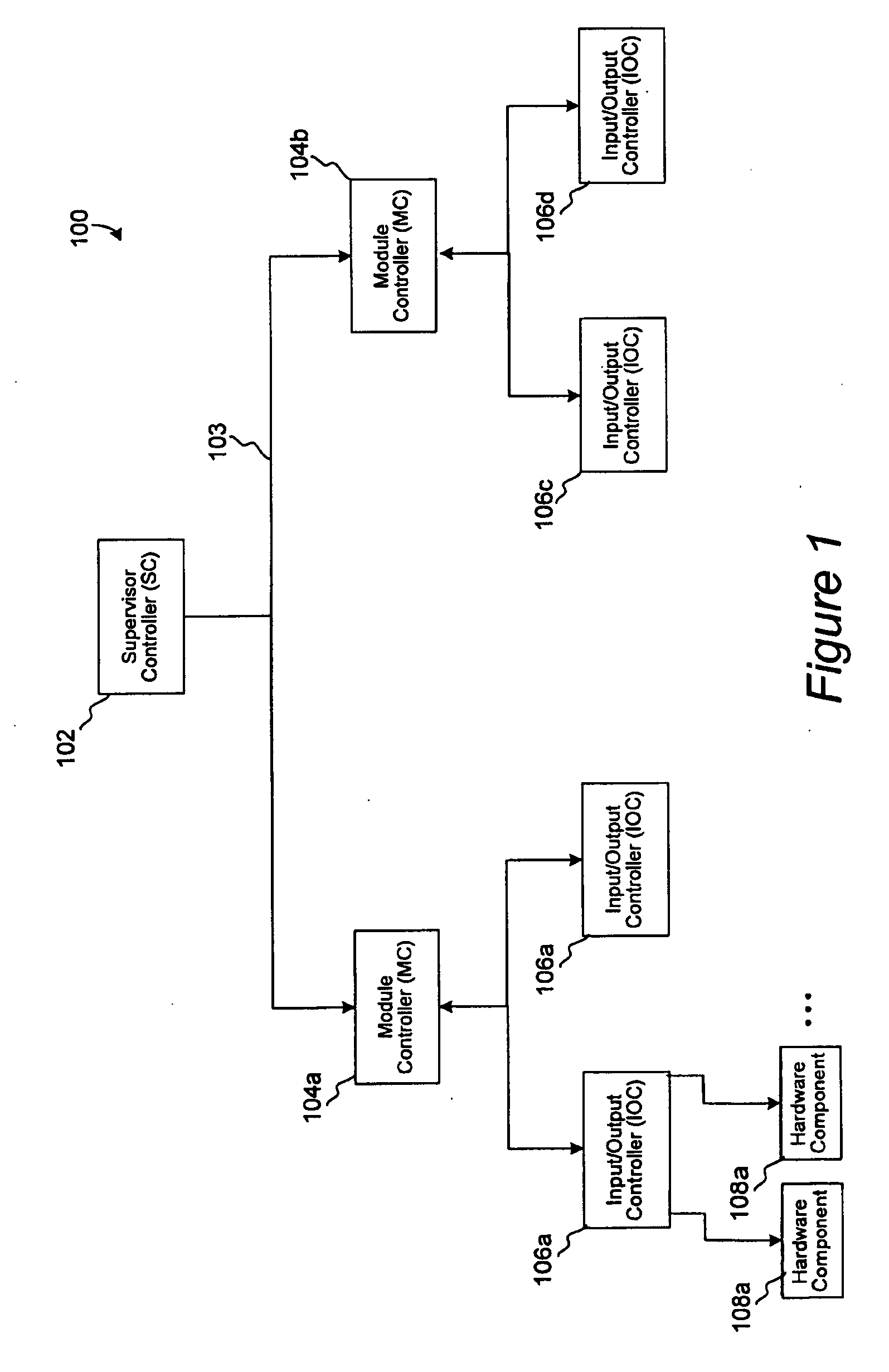
[0018]Embodiments of the present invention are particularly useful in a distributed control system for con...


PUM


Abstract

Disclosed are apparatus and methods for embodiments for efficiently and flexibly controlling hardware devices in a semiconductor processing system are provided for use in a distributed control arrangement. In general, the distributed arrangement includes at least one upper-level controller that is configurable with a computer program sequence of instructions for controlling one or more hardware devices of a processing tool. The hardware devices are controlled through one or more lower-level controllers. Prior to execution of the program sequence of the upper-level controller, at least one instruction of this program is pre-compiled so as to translate the instruction for execution by a selected lower-level controller and to add an at least one interlock check to such pre-compiled instruction and make the translated instruction accessible to at least one lower-level controller. The interlock check specifies one or more condition(s) for the selected lower-level controller to execute the pre-compiled instruction. Any number of instructions of the upper-level controller may be translated for use by any number of selected lower-level controllers, where some of the translated instructions include one or more interlock checks.

Description

CROSS REFERENCE TO RELATED PATENT APPLICATION[0001]This application is a continuation of and claims priority of U.S. patent application Ser. No. 11 / 556,989, entitled APPARATUS AND METHODS FOR PRECOMPILING PROGRAM SEQUENCES FOR WAFER PROCESSING, filed 6 Nov. 2006 by Jaideep Jain et al., which application is incorporated herein by reference in its entirety for all purposes.BACKGROUND OF THE INVENTION [0002]The present invention relates generally to processing of semiconductor wafers in a plurality of processing systems. More specifically, it relates to computer programs for controlling the operation of devices in such processing systems.[0003]Generally, the industry of semiconductor manufacturing involves highly complex techniques for fabricating integrating circuits from semiconductor materials that are layered and patterned onto a substrate, such as silicon, by various process systems. For example, a first process system deposits a layer of material, while another process system etc...

Claims


Application Information

Patent Timeline
Patent Type & Authority Applications(United States)
IPC IPC(8): G05B15/02G06F9/455G05D7/00G05B9/02G05B17/02G06G7/66
CPCG05B19/4148G05B2219/45031G05B2219/33104
Inventor JAIN, JAIDEEPZHOU, QIANGKLEINKE, STEVE
Owner NOVELLUS SYSTEMS
Why Eureka
Try Eureka