Method of designing semiconductor device

a semiconductor chip and design technology, applied in semiconductor devices, semiconductor/solid-state device details, electrical devices, etc., can solve the problems of inability to completely eliminate the accuracy variation between manufacturing devices, the mixing of foreign substances, and the like in the manufacturing process of semiconductor devices, and the scattered semiconductor chips of defective parts therein. the effect of yield rate and yield rate in the manufacture of semiconductor integrated circuits

Inactive Publication Date: 2009-05-28
RENESAS ELECTRONICS CORP
View PDF1 Cites 0 Cited by
  • Summary
  • Abstract
  • Description
  • Claims
  • Application Information

AI Technical Summary

Benefits of technology

[0011]Since macro test information is created by carrying out tests in the phase of a base wafer in such a manner, a yield rate in the manufacture of semiconductor integrated circuits, especially structured ASICs can be improved.
[0012]A yield rate in the manufacture of semiconductor integrated circuits can be improved.

Problems solved by technology

Furthermore, ASICs have been also well known as ICs that are used for specific applications and must be produced in large volume even though they are large-scale circuits and designing them is quite difficult.
Meanwhile, it is impossible to completely eliminate accuracy variation between manufacturing devices, the mixing of foreign substances, and the like in a manufacturing process of semiconductor devices.
Such variation between manufacturing devices and a mixing of foreign substances may result in semiconductor chips having a defective portion therein scattered over the wafer.
However, Okamoto discloses merely a technique to summarize test results, and does not give any thought to improvements in a yield rate of structured ASICs like the ones described above.
In a structured ASIC like the one described above, since circuits corresponding to various function macros are built into the chip in advance, the preventive provision of the circuits that are used to substitute for a circuit when the circuit is found to be defective in a similar manner to the redundant cells may wastefully increase the circuit area.

Method used


Image

  • Method of designing semiconductor device
  • Method of designing semiconductor device
  • Method of designing semiconductor device

Examples


Embodiment Construction

[0025]Exemplary embodiments in accordance with the present invention are explained hereinafter with reference to the drawings. FIGS. 1, 2, 3, and 4 show schematic diagrams, flowcharts, and the likes for illustrating an exemplary embodiment in accordance with the present invention. In the following explanations, exemplary embodiments in accordance with the present invention are explained by using FIGS. 1-4 as appropriate.

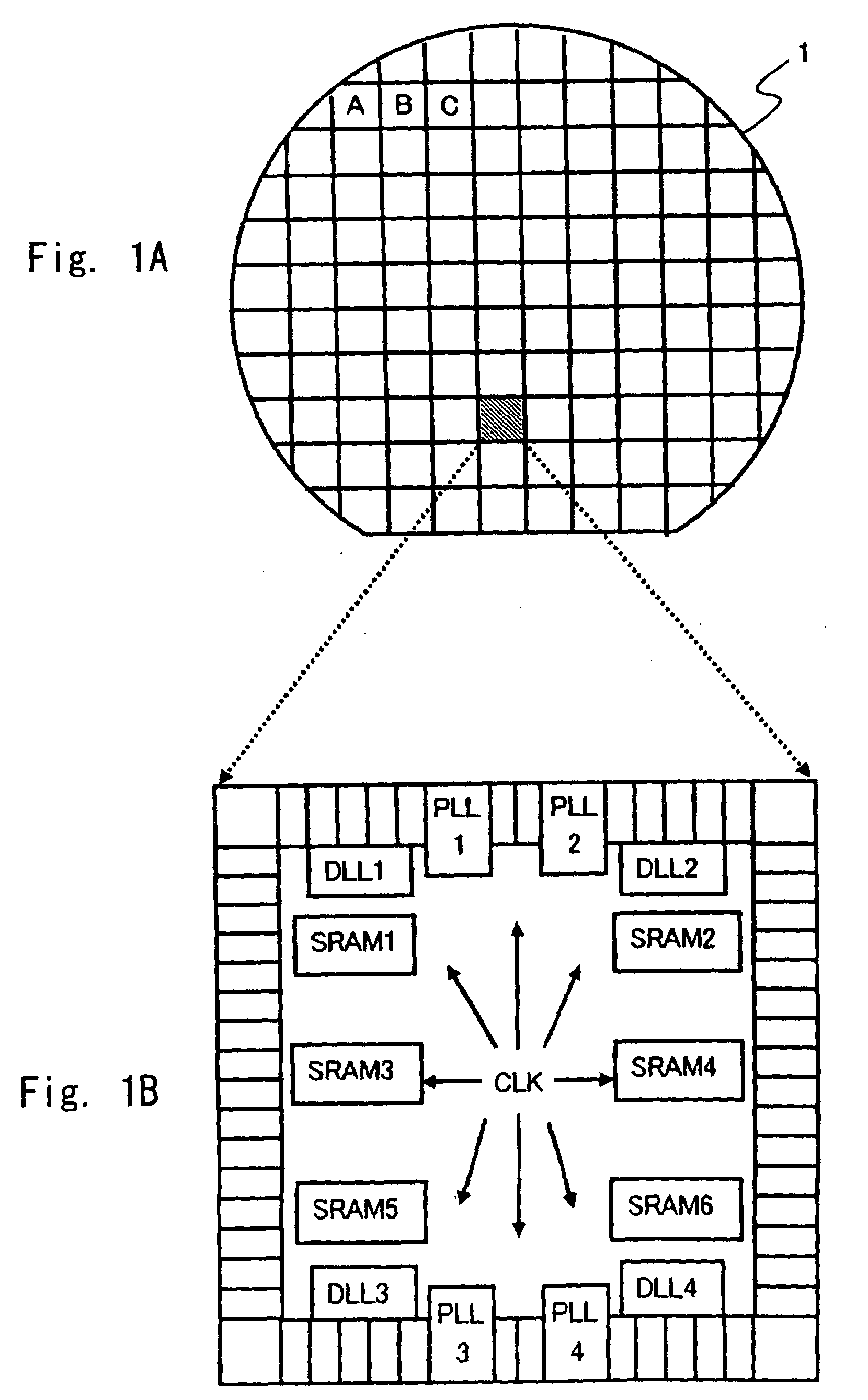
[0026]In an exemplary embodiment in accordance with the present invention, a plurality of wafers (which are called “base wafers” hereinafter) 1 are first prepared in a state before the manufacture of semiconductor devices using a structured ASIC technique is completed. This base wafer 1 is a kind of wafer in which various elements, logic gates, and the likes formed on the semiconductor substrate are connected by several wiring layers formed on the semiconductor substrate in order to form a plurality of function macros (which is also called “macros” hereinafter) and f...


PUM


Abstract

A design method of a semiconductor device comprising forming a base wafer by using a plurality of semiconductor chips including a plurality of functional macros, generating macro test information by testing the plurality of function macros of the plurality of semiconductor devices; and picking a macro that is prohibited from being used out of the plurality of function macros based on the macro test information and a net list of user circuit. Since tests are carried out at the phase of a base wafer, it is possible to improve yield rates in the manufacture of semiconductor integrated circuits.

Description

BACKGROUND[0001]1. Field of the Invention[0002]The present invention relates to a method of designing a semiconductor device. In particular, the present invention relates to a method of designing a structured ASIC (Application Specific Integrated Circuit) in which a desired semiconductor device having various functions is designed by designing a wiring layer for the semiconductor device on which a plurality of function macros and function cells are previously embedded.[0003]2. Description of Related Art[0004]FPGAs (Field Programmable Gate Arrays) have been well known as devises that are developed in a short period and can be re-programmed in the field of semiconductor devices. Furthermore, ASICs have been also well known as ICs that are used for specific applications and must be produced in large volume even though they are large-scale circuits and designing them is quite difficult. In recent years, semiconductor devices called “structured ASICs” have become widespread as intermedia...

Claims


Application Information

Patent Timeline
Patent Type & Authority Applications(United States)
IPC IPC(8): H01L23/02H01L21/50
CPCH01L23/585H01L27/0207H01L2924/0002H01L2924/00
Inventor KONDOU, KEIICHIROU
Owner RENESAS ELECTRONICS CORP
Why Eureka
Try Eureka