
LED package, and illumination device and liquid crystal display device provided therewith

a technology of illumination device and which is applied in the direction of lighting support device, lighting and heating apparatus, instruments, etc., can solve the problems of degrading the display quality of the liquid crystal display device, affecting the brightness and color of light emanating from the emission surface,

Inactive Publication Date: 2009-05-28
SHARP KK
View PDF16 Cites 22 Cited by
  • Summary
  • Abstract
  • Description
  • Claims
  • Application Information

AI Technical Summary

Benefits of technology

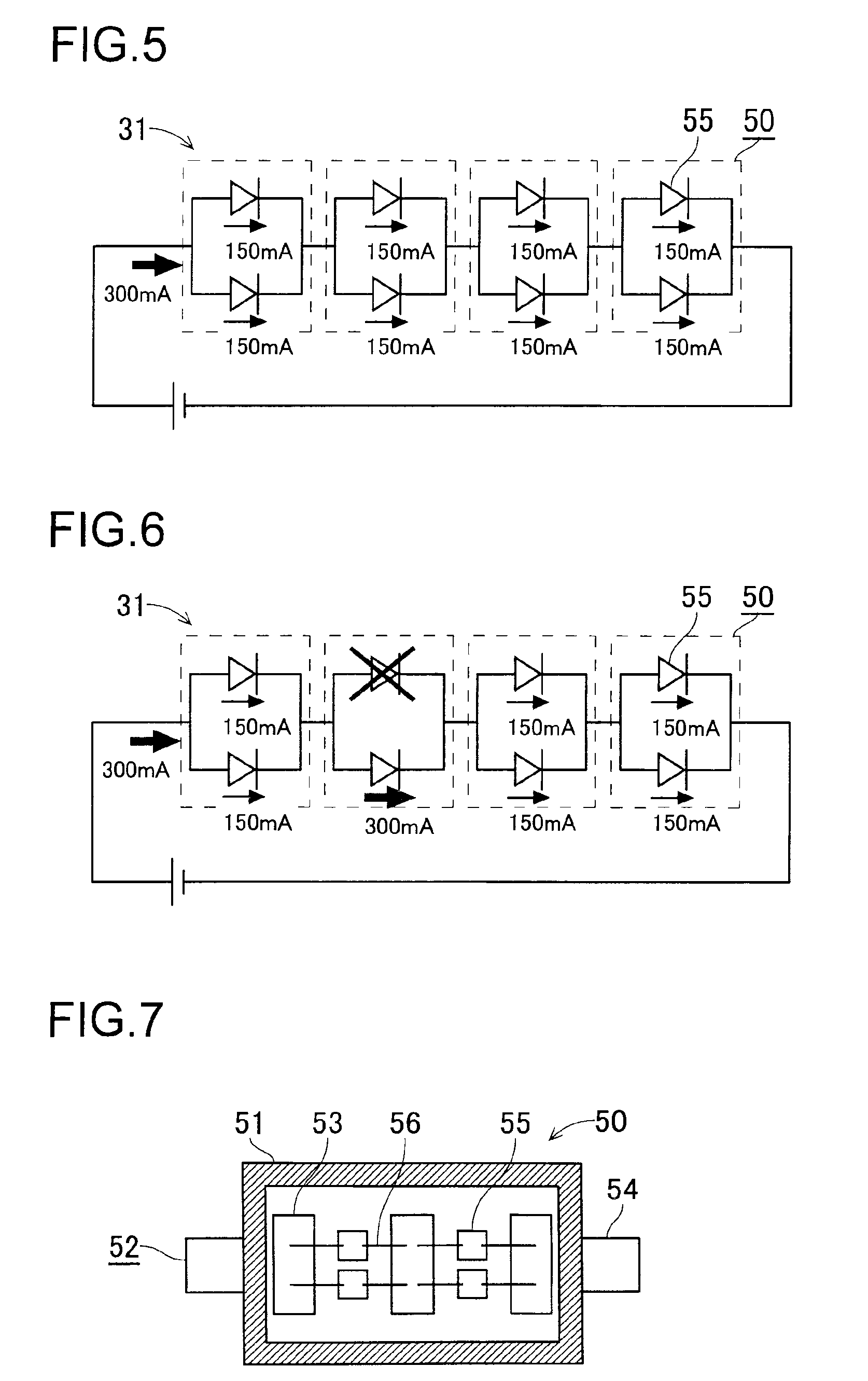
[0007]In order to overcome the problems described above, preferred embodiments of the present invention provide an LED package that can maintain its lit state and can maintain the amount of light emitted even when an open circuit failure occurs in an LED chip, and provide an illumination device for use in a liquid crystal display device in which variations in the brightness and color of light emitted are less likely to occur even when an open circuit failure occurs in an LED package.

Problems solved by technology

Incidentally, in a case where a wire bonded to an LED chip is broken, and thus an open circuit failure or other failures occur and this causes the LED packages disposed on the side of the light guide plate to become unlit, variations in the brightness and color of light emanating from the emission surface occur.
Such variations in the brightness and color of backlight affect the display of the liquid crystal panel, with the result that the display quality of the liquid crystal display device is degraded.

Method used


Image

  • LED package, and illumination device and liquid crystal display device provided therewith
  • LED package, and illumination device and liquid crystal display device provided therewith
  • LED package, and illumination device and liquid crystal display device provided therewith

Examples


first preferred embodiment

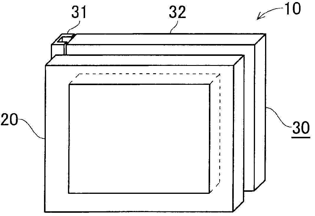
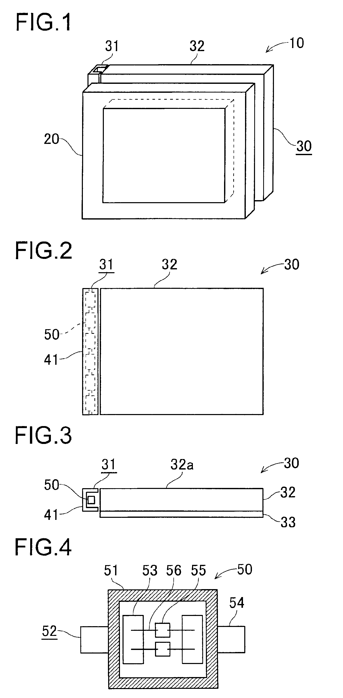
[0031]A first preferred embodiment of the present invention will be described with reference to the accompanying drawings. FIG. 1 is a diagram schematically showing the configuration of a liquid crystal display device according to the first preferred embodiment. FIG. 2 is a plan view of a backlight according to the first preferred embodiment. FIG. 3 is a front view of the backlight according to the first preferred embodiment. FIG. 4 is a diagram schematically showing the configuration of an LED package according to the first preferred embodiment.

[0032]As shown in FIG. 1, the liquid crystal display device 10 has a liquid crystal panel 20 and the backlight 30 serving as an illumination device. The liquid crystal panel 20 has a TFT substrate, an opposite substrate and liquid crystal sealed in therebetween. The orientation of the liquid crystal is controlled by applying voltage to both the substrates, and this allows an image to be displayed. The backlight 30 is disposed on the back of ...

second preferred embodiment

[0038]A second preferred embodiment of the present invention will be described with reference to the accompanying drawings. FIG. 7 is a diagram schematically showing the configuration of an LED package according to the second preferred embodiment. The second preferred embodiment is the same as the first preferred embodiment except that the configuration of the light emission section is different from each other, and such parts as are substantially the same as each other are identified with common reference numerals.

[0039]As shown in FIG. 7, the LED package 50 of this preferred embodiment has a frame 51 and a light emission section 52. The light emission section 52 has three lead frames 53, two disposed at both ends of the frame 51 and the other disposed in the middle thereof inside the frame 51, terminals 54 connected to the lead frames 53 at both ends and four LED chips 55. Between the lead frames 53 at both ends and the lead frame 53 in the middle, two LED chips 55 are individuall...

third preferred embodiment

[0043]A third preferred embodiment of the present invention will be described with reference to the accompanying drawings. FIG. 8 is a diagram schematically showing the configuration of an LED package according to the third preferred embodiment. The third preferred embodiment is the same as the second preferred embodiment except that the LED package 50 has three light emission sections, and the three light emission sections have LED chips emitting red (R), green (G) and blue (B) light, respectively and such parts as are substantially the same as each other are identified with common reference numerals.

[0044]As shown in FIG. 8, the LED package 50 of this preferred embodiment has a frame 51 and the three light emission sections 52R, 52G and 52B. Each of the light emission sections 52R, 52G and 52B has two lead frames 53, terminals 54 connected to the lead frames 53 and two LED chips emitting red (R), green (G) or blue (B) light.

[0045]In the light emission sections 52R, 52G and 52B, th...


PUM


Abstract

In an LED package, LED chips are connected in parallel by wires between lead frames connected to terminals. When an open circuit failure such as the coming off of the wire occurs in one of the LED chips in the LED package that is being energized, a current twice as high as that flowing through the other LED chip prior to the open circuit failure is passed through the other LED chip, and thus the amount of light emitted therefrom is increased about two-fold. Consequently, the amount of light emitted from the LED package does not change significantly.

Description

BACKGROUND OF THE INVENTION[0001]1. Field of the Invention[0002]The present invention relates to an LED package, and an illumination device and a liquid crystal display device incorporating such an LED package.[0003]2. Description of the Related Art[0004]In recent years, products that incorporate, as a display device, a liquid crystal panel thinner than a CRT (cathode ray tube) have been widely used. Since the liquid crystal panel itself emits no light, it displays an image by the use of external light or light emitted from an illumination device.[0005]One example of an illumination device for use in a liquid crystal display device is a sidelight backlight proposed in JP-A-2004-021147 (pages 4 and 5, FIG. 1). This illumination device is disposed at the back side of a liquid crystal panel. In the illumination device, on the side of a flat plate called a light guide plate formed of acrylic resin, LED (light emitting diode) packages are disposed as a light source; light from the LED pa...

Claims


Application Information

Patent Timeline
Patent Type & Authority Applications(United States)
IPC IPC(8): F21V8/00F21V21/00H01L33/62
CPCG02F1/133603G02F1/133615G02F2001/133612H01L2224/49113H01L33/62H04M1/22H01L25/0753G02F1/133612
Inventor HAMADA, TETSUYA
Owner SHARP KK
Learn More