Separate testing of continuity between an internal terminal in each chip and an external terminal in a stacked semiconductor device

a technology of stacked semiconductor devices and continuity testing, which is applied in the direction of semiconductor/solid-state device testing/measurement, semiconductor/solid-state device details, instruments, etc., can solve the problems of inability to identify the chip with a defective connection, continuity testing cannot be conducted, and cannot be seen

Inactive Publication Date: 2009-06-18
LONGITUDE LICENSING LTD
View PDF10 Cites 26 Cited by
  • Summary
  • Abstract
  • Description
  • Claims
  • Application Information

AI Technical Summary

Benefits of technology

[0017]It is an object of the present invention to provide a stacked semiconductor device which is capable of conducting a test to determine whether or not there is continuity between an external terminal and a corresponding internal terminal in each chip, on an internal terminal-in each chip basis.

Problems solved by technology

As a result, even if a chip having a defective connection is present, it is difficult to identify the chip having a defective connection.
Therefore, a continuity test cannot be conducted because the internal terminal junction cannot be seen as the external terminal.
As a result, whether or not there are defects in the connection between chips cannot be seen until a test to determine whether or not the circuits in a semiconductor package operate properly, is conducted, and cannot be easily found prior to testing the operation of the circuits.

Method used


Image

  • Separate testing of continuity between an internal terminal in each chip and an external terminal in a stacked semiconductor device
  • Separate testing of continuity between an internal terminal in each chip and an external terminal in a stacked semiconductor device
  • Separate testing of continuity between an internal terminal in each chip and an external terminal in a stacked semiconductor device

Examples


first exemplary embodiment

[0029]FIG. 3 illustrates the detailed configuration of an input / output section of a semiconductor device according to a first exemplary embodiment of the present invention.

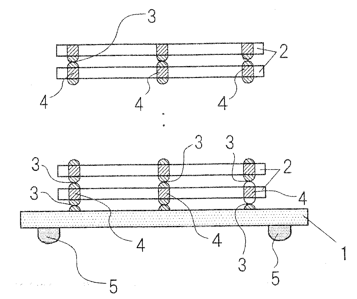
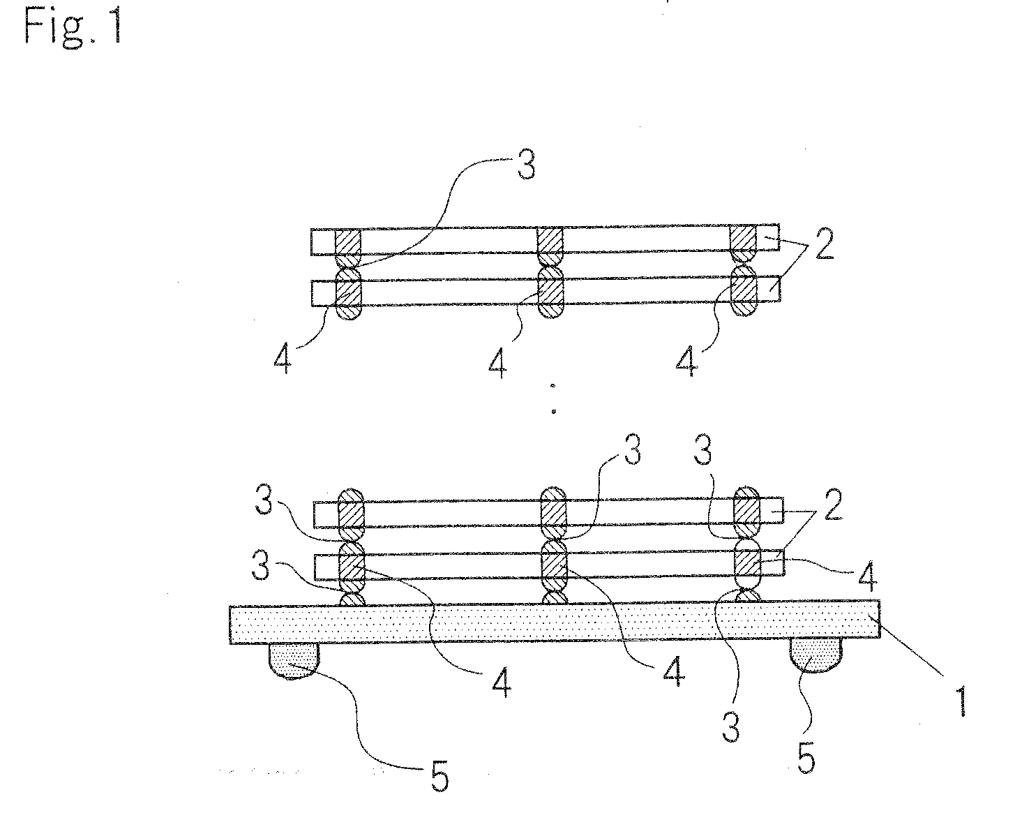
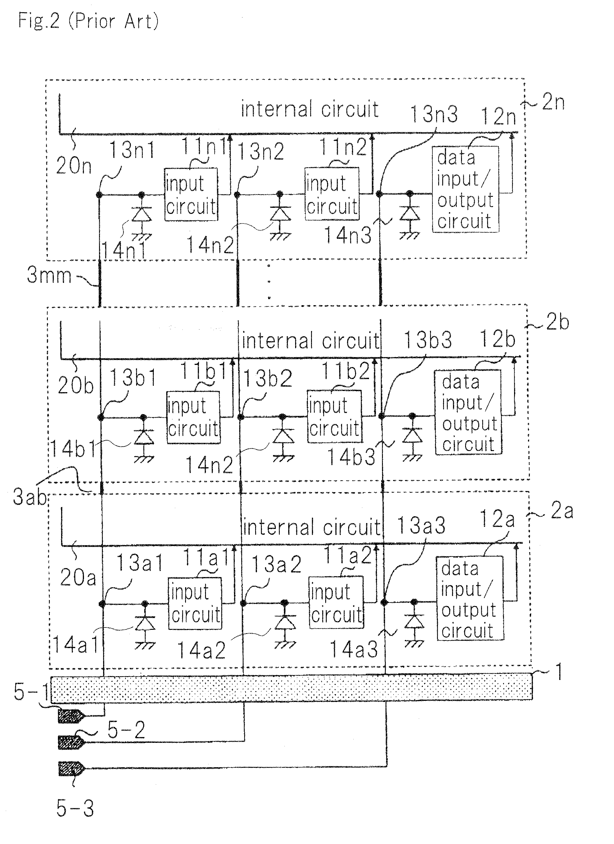
[0030]This stacked semiconductor includes interposer chip 1, a plurality of identical chips 2a, 2b, 2c, . . . that are stacked on interposer chip 1, external terminals 5-1, 5-2, 5-3, . . . , and continuity test dedicated terminals 6a, 6b, 6c, . . . , each associated with memory core chips 6a, 6b, 6c, . . . , respectively, continuity test dedicated terminals 6a, 6b, 6c each associated with memory core chips 6a, 6b, 6c, respectively.

[0031]Memory core chip 2a includes internal circuit 20a, input circuit 11a1, 11a2, data input / output circuit 12a; internal terminal 13a1, 13a2 for providing input circuit 11a1, 11a2 with a signal to operate internal circuit 20a, respectively, internal terminal 13a3 for inputting data to data input / output circuit 12a and for outputting data from data input / output circuit 12a. Similarly, m...

second exemplary embodiment

[0041]FIGS. 4a, 4b illustrate schematic configurations of another stacked semiconductor devices. The stacked semiconductor devices illustrated in FIGS. 4a, 4b differ from the stacked semiconductor device illustrated in FIG. 1 in that chips to be stacked include different chips (in this case, a memory core chip and an interface chip). FIG. 4a is an example in which the number of memory core chip 2 is one, and FIG. 4b is an example in which the number of memory core chip 2 is two. Interface chip 7 is a semiconductor chip which performs a specific circuit operation. Internal signals in memory core chip 2 and interface chip 7 communicate therebetween via internal terminal junction 3.

[0042]FIG. 5 illustrates the detailed configuration of an input / output section of a semiconductor device according to a second exemplary embodiment. This exemplary embodiment is applied to the semiconductor device shown in FIG. 4b. The configurations of memory core chips 2a, 2b and 2c are the same as those o...

third exemplary embodiment

[0047]FIG. 6a illustrates the detailed configuration of an input / output section of a semiconductor device according to a third exemplary embodiment. This exemplary embodiment is also applied to the semiconductor device shown in FIG. 4b. The present exemplary embodiment differs from the second exemplary embodiment in that external terminals 5-1, 5-2 for inputting control signals necessary for the control of internal circuit 20 in interface chip 7 are also used as external terminals to check the connection status of the internal terminals in memory core chip 2a. This reduces the number of external terminals of the stacked semiconductor device.

[0048]The detailed configuration will be described below. Interface chip 7 includes continuity test control terminal 6 and transfer gates 18-1, 18-2. In order to suppress ESD that is caused through continuity test control terminal 6, continuity test control terminal ESD element 21 is provided. Transfer gates 18-1 and 18-2 are of a conventional ci...


PUM


Abstract

A stacked semiconductor device is disclosed which is capable of conducting a test to determine whether or not there is continuity between an external terminal and a corresponding internal terminal in each chip, on an internal terminal-in each chip basis. The semiconductor device includes continuity test dedicated terminals for each chip, and continuity test elements each connected between an internal terminal in each chip and a continuity test dedicated terminal associated with the chip. A voltage is applied between an external terminal associated with an internal terminal whose connection status is to be checked and a continuity test dedicated terminal associated with a chip which includes the internal terminal such that a continuity test element associated with the internal terminal is rendered conductive. Thereafter, the value of current that flows through the continuity test element is measured to determine the connection status of the internal terminal.

Description

[0001]This application is based upon and claims the benefit of priority from Japanese patent application No. 2007-317078 filed on Dec. 7, 2007, the disclosure of which is incorporated herein in its entirety by reference.BACKGROUND OF THE INVENTION[0002]1. Field of the Invention[0003]The present invention relates to a stacked semiconductor device wherein a plurality of different or identical chips are stacked using through-hole electrodes, and more particularly to a method of testing continuity between an internal terminal in each chip and an external terminal.[0004]2. Description of the Related Art[0005]In recent years, semiconductor packages wherein a plurality of chips are stacked using through-hole electrodes have been developed (see, for example, JP2002-305283A).[0006]FIG. 1 illustrates an exemplary configuration of a semiconductor package wherein a plurality of memory core chips and an interposer chip are stacked together.[0007]A signal which is applied to external terminal 5 i...

Claims


Application Information

Patent Timeline
Patent Type & Authority Applications(United States)
IPC IPC(8): G01R31/26H01L23/52
CPCG01R31/31717G01R31/318513G11C5/02G11C5/04G11C29/02G11C29/022H01L2924/15311H01L22/32H01L25/0657H01L2224/16145H01L2225/06513H01L2225/06541H01L2225/06596G11C29/025H01L2224/05573H01L2224/13025H01L2924/00014H01L2224/05599
Inventor SHIBATA, KAYOKO
Owner LONGITUDE LICENSING LTD
Why Eureka
Try Eureka