Electrically-Driven Liquid Crystal Lens and stereoscopic Display Device Using the Same

a liquid crystal lens and electric drive technology, applied in the direction of instruments, color television details, electrical equipment, etc., can solve the problems of adhesive use, deterioration of transmissivity, and image quality degradation

Active Publication Date: 2009-06-18
LG DISPLAY CO LTD
View PDF13 Cites 64 Cited by
  • Summary
  • Abstract
  • Description
  • Claims
  • Application Information

AI Technical Summary

Benefits of technology

[0023]An object of the present invention is to provide an electrically-driven liquid crystal lens wherein electric connection between finely split electrodes and signal lines used to apply signals to the split ele

Problems solved by technology

This bending phenomenon results in abnormal optical pathways through the backlight unit 20, liquid crystal panel 10, and lenticular plate 30, thereby deteriorating image quality.
Moreover, the adhesive problematically causes deterioration in transmissivity.
Other problems associated with the attachment of the above-described lenticular lens include the use of the adhesive, deteriorated visual sensitivity due to the bending phenomenon, or a difficulty in the processing of a smooth lenticular lens.
In

Method used


Image

  • Electrically-Driven Liquid Crystal Lens and stereoscopic Display Device Using the Same
  • Electrically-Driven Liquid Crystal Lens and stereoscopic Display Device Using the Same
  • Electrically-Driven Liquid Crystal Lens and stereoscopic Display Device Using the Same

Examples


first embodiment

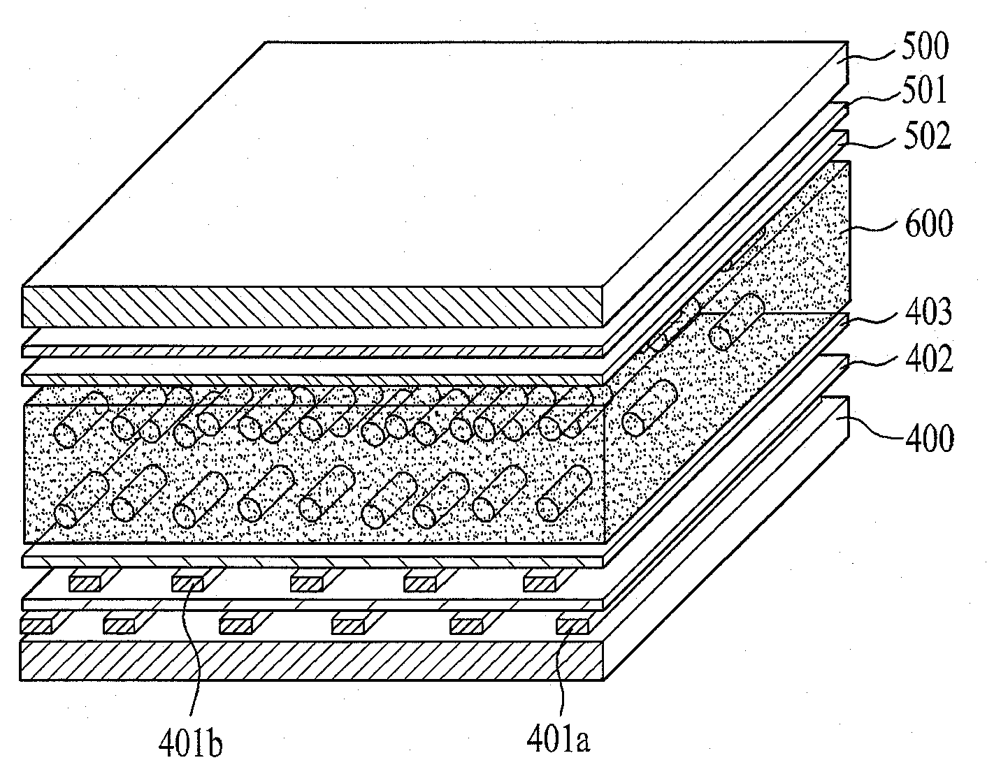
[0073]Although not described, in the drawings, reference numeral 403 represents a first alignment film, reference numeral 500 represents a second substrate, and reference numerals 501 and 502 represent a second electrode and a second alignment film, respectively. Also, reference numeral 600 represents a liquid crystal layer. These constituent elements have the same functions as those of the above-described first embodiment, and a description thereof will be omitted.

[0074]With the above-described configuration as shown in FIGS. 6 and 7 in which the first electrodes 401a and 401b associated with the first substrate 400 of the electrically-driven liquid crystal lens are formed on the two layers, more dense and close arrangement of electrodes is possible, resulting in a lens profile more similar to a parabolic lens than the above-described profile shown in FIG. 5.

[0075]Hereinafter, a method for applying signals to the respective electrodes of the electrically-driven liquid crystal lens ...

second embodiment

[0099]Hereinafter, a method for forming contacts between electrodes and metal lines using a reduced number of masks will be described.

[0100]FIGS. 14A to 14D are process sectional views illustrating a method for forming electrodes and metal lines according to a second embodiment of the present invention, FIGS. 15A to 15D are sequential process sectional views taken along the line III-III′ of FIG. 14C, and FIGS. 16A and 16B are sequential process sectional views taken along the line IV-IV′ of FIG. 14C.

[0101]In the drawings, of pad regions on a first substrate, only a particular pad region, located at the upper side or lower side of a first substrate in which contacts between electrodes and metal lines are formed, is illustrated.

[0102]To form electrodes and signal lines according to the second embodiment of the present invention, first, as shown in FIGS. 14A and 15A, after depositing metal on the first substrate 400, the deposited metal is selectively removed, forming metal lines 430....

third embodiment

[0111]FIG. 17 is a plan view illustrating an electrically-driven liquid crystal lens according to the present invention.

[0112]As shown in FIG. 17, in consideration of the fact that the longer the length of first electrodes or metal lines, the greater the line resistance, the electrically-driven liquid crystal lens according to the third embodiment of the present invention proposes to prevent a location away from a signal applying location from receiving an incorrect voltage, causing deterioration in reliability.

[0113]For this, in the third embodiment, a first substrate 800 is divided into a plurality of sections A, B, C and D, and the sections A, B, C and D are provided with first electrodes 811, 812, 813 and 814, respectively and also, are provided with metal lines 831, 832, 833 and 834 to be brought into contact with the respective first electrodes 811, 812, 813 and 814, respectively.

[0114]In the above-described configuration, assuming that n voltages are applied to the metal line...


PUM


Abstract

An electrically-driven liquid crystal lens wherein electric connection between finely split electrodes and signal lines used to apply signals to the split electrodes can be accomplished using a minimal number of masks and signals can be applied to the finely split electrodes without line resistance, and a stereoscopic display device using the same are disclosed. The liquid crystal lens includes first and second substrates arranged opposite each other and each defining a plurality of lens regions, a plurality of metal lines formed on the first substrate, a first insulating film formed on the first substrate, a plurality of first electrodes formed on the first insulating film in the respective lens regions to intersect the plurality of metal lines, a second insulating film formed on the first electrodes, a plurality of second electrodes formed on the second insulating film at positions alternating with the first electrodes, a first contact structure between the first electrodes and the metal lines using a transparent electrode pattern of the same layer as the second electrodes, a second contact structure between the second electrodes and the plurality of metal lines, a common electrode formed over the entire surface of the second substrate, and a liquid crystal layer filled between the first substrate and the second substrate.

Description

[0001]This application claims the benefit of the Korean Patent Application No. P2007-130926, filed on, Dec. 14, 2007, which is hereby incorporated by reference as if fully set forth herein.BACKGROUND OF THE INVENTION[0002]1. Field of the Invention[0003]The present invention relates to a stereoscopic display device, and more particularly, to an electrically-driven liquid crystal lens wherein electric connection between finely split electrodes and signal lines used to apply signals to the split electrodes can be accomplished using a minimal number of masks and wherein signals can be applied to the finely split electrodes without the effect of line resistance, and a stereoscopic display device using the same.[0004]2. Discussion of the Related Art[0005]At present, services for rapid dissemination of information, constructed on the basis of high-speed information communication networks, have developed from a simple “listening and speaking” service, such as current telephones, to a “watch...

Claims


Application Information

Patent Timeline
IPC IPC(8): H04N13/04G02B30/28
CPCG02F1/1345G02F1/13471G02B27/2214G02B3/14G02F2001/134381G02F1/134381G02B30/28G02F1/1335G02B26/00G02B30/27
Inventor LEE, BYUNG JOOIM, HEE JIN
Owner LG DISPLAY CO LTD
Why Eureka
Try Eureka