Thin film transistor substrate having low resistance bus line structure and method for manufaturing the same

a thin film transistor and bus line structure technology, applied in the field of thin film transistors (or “ tft”) substrates having a low resistance bus line structure, can solve the problems of reduced aperture ratio of display area, difficult selection of materials having a lower resistivity, and video quality problems of display devices, etc., to achieve low resistance of bus lines, reduce or maintain resistance of bus lines in a lower state, and reduce cross-sectional area

Active Publication Date: 2012-01-12
LG DISPLAY CO LTD
View PDF7 Cites 23 Cited by
  • Summary
  • Abstract
  • Description
  • Claims
  • Application Information

AI Technical Summary

Benefits of technology

[0034]In the thin film transistor substrate for the flat panel display device according to the present disclosure, the bus lines are formed thicker than those of related art, but the bus lines are buried in the substrate. Therefore, the cross-sectional area of the bus lines can be larger than that of the related art, and the resistance of the bus lines can be reduced or maintained in lower state. Furthermore, as the thick bus lines are buried into the substrate, there...

Problems solved by technology

The LCD according to the related art explained above has a problem regarding a large display area.
As a result, the display device has video quality problems.
To select a material having a lower resistivity is very difficult because the mater...

Method used


Image

  • Thin film transistor substrate having low resistance bus line structure and method for manufaturing the same
  • Thin film transistor substrate having low resistance bus line structure and method for manufaturing the same
  • Thin film transistor substrate having low resistance bus line structure and method for manufaturing the same

Examples


Embodiment Construction

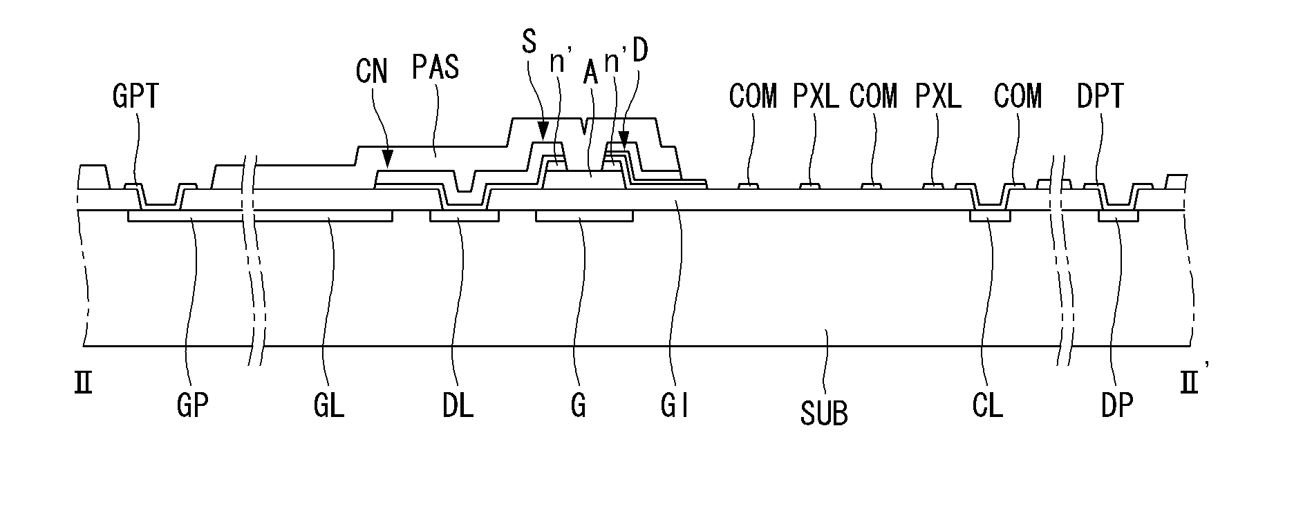
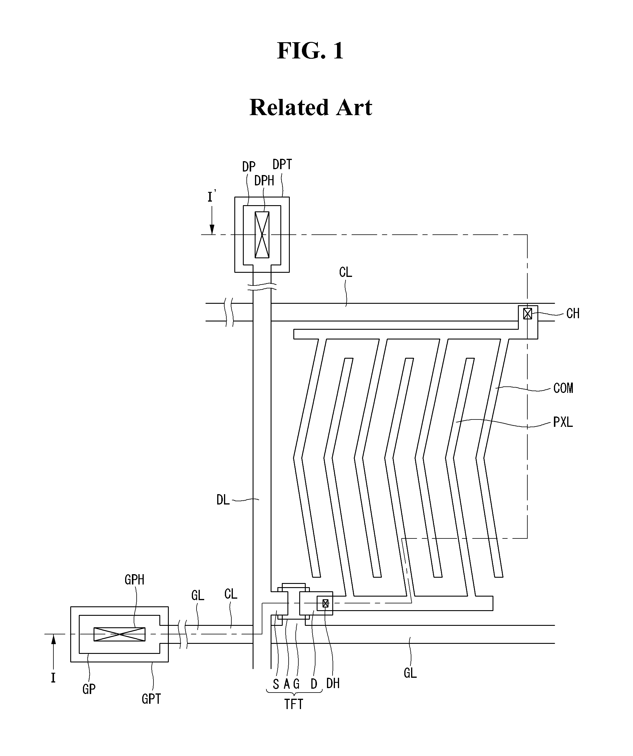
[0041]Referring to attached figures including FIG. 3 and FIGS. 4A to 4E, we will explain preferred embodiments of the present disclosure. FIG. 3 is a plane view illustrating the structure of a thin film transistor substrate having a low resistance bus line structure used in a horizontal electric field type liquid crystal display device according to the present disclosure. FIGS. 4A to 4E are cross-sectional views illustrating the steps of manufacturing for the thin film transistor substrate having a low resistance bus line structure of FIG. 3 by cutting along the line II-II′, according to present disclosure.

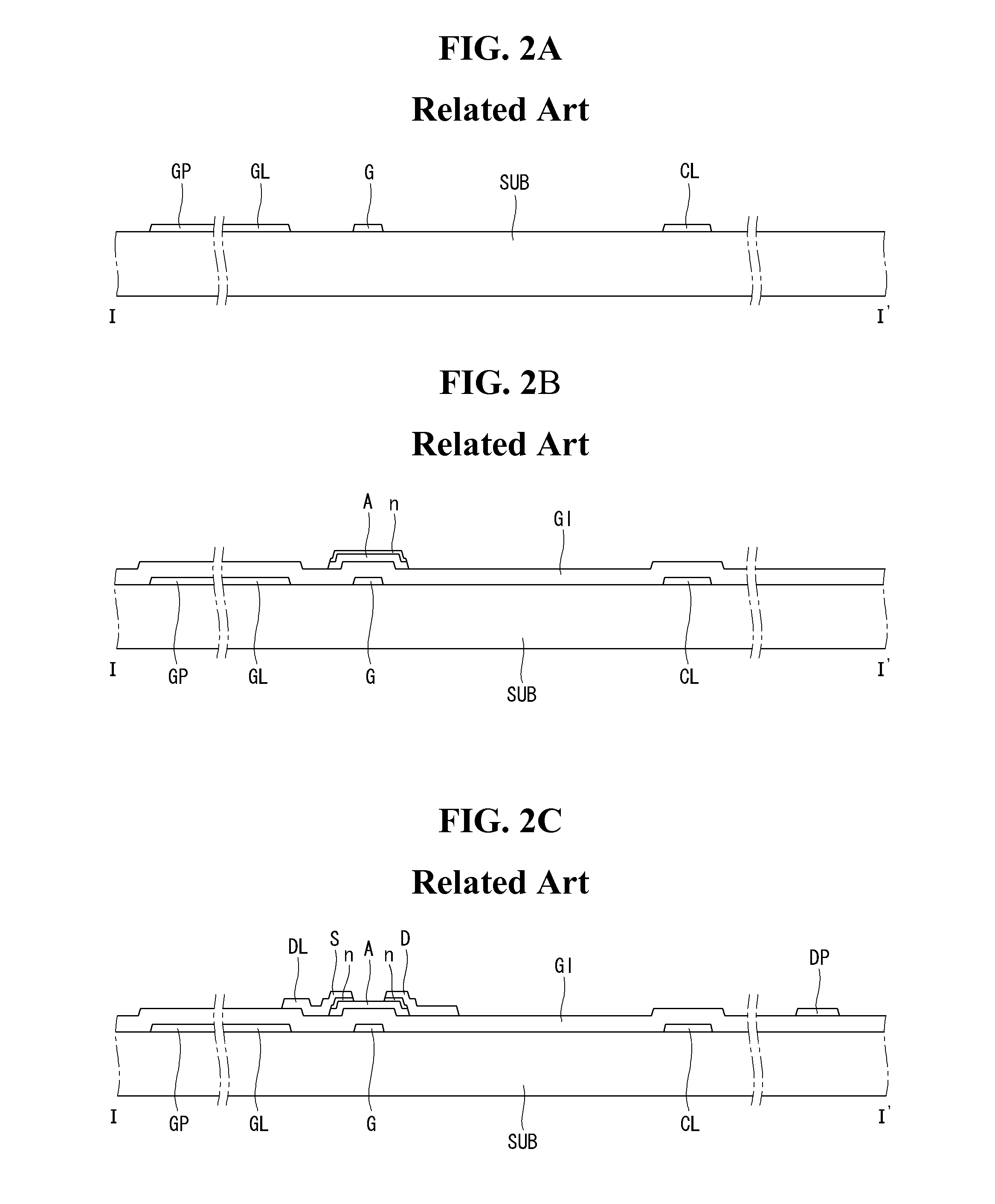
[0042]Referring to FIG. 3 and FIGS. 4A to 4E, the thin film transistor substrate for an LCD comprises a gate line GL and a data line DL which are crossing each other with a gate insulating layer therebetween on a glass substrate SUB, and a thin film transistor TFT formed at the crossing portion of the gate line GL and the data line DL. The crossing gate line GL and the data line D...


PUM


Abstract

A method for manufacturing a thin film transistor substrate including forming bus lines by etching a surface of a substrate to form bus line patterns and filling the bus line patterns with a bus line metal; forming a semiconductor channel layer at one portion of a pixel area defined by the bus lines; and forming source-drain electrodes on the semiconductor channel layer, a pixel electrode extending from the drain electrode within the pixel area, and a common electrode parallel with the pixel electrode. The bus lines are formed as being thicker but the bus lines are buried in the substrate so that the line resistance can be reduced and the step difference due to the thickness of bus line does not affect the device.

Description

[0001]This application claims the benefit of Korean Patent Application No. 10-2010-0065239 filed on Jul. 7, 2010, which is incorporated herein by reference for all purposes as if fully set forth herein.BACKGROUND OF THE INVENTION[0002]1. Field of the Invention[0003]The present disclosure relates to a thin film transistor (or “TFT”) substrate having a low resistance bus line structure and a method for manufacturing the same. Particularly, the present disclosure relates to a TFT substrate having a thick bus line buried in a substrate having a low resistance bus line structure and a method for manufacturing the same.[0004]2. Discussion of the Related Art[0005]Various flat panel display devices are developed to overcome many drawbacks of the cathode ray tube such as heavy weight and bulky volume. The flat panel display devices include the liquid crystal display device (or LCD), the field emission display (or FED), the plasma display panel (or PDP) and the electroluminescence device (or ...

Claims


Application Information

Patent Timeline
IPC IPC(8): H01L29/786H01L21/336
CPCG02F1/136286H01L27/124H01L27/1218H01L27/1214
Inventor LEE, JUNGILCHUNG, INJAEYANG, JOONYOUNGHONG, GISANG
Owner LG DISPLAY CO LTD
Why Eureka
Try Eureka