Transparent capacitive touch panel and manufacturing method thereof

a technology manufacturing method, which is applied in the field of touch panel, can solve the problems of reducing the manufacturing yield of transparent capacitive touch panel, complicated manufacturing process, and indium-tin oxide layer, and achieves the effects of simplified manufacturing process, simplified manufacturing process, and high manufacturing yield

Active Publication Date: 2009-06-25
TPK HLDG
View PDF12 Cites 116 Cited by
  • Summary
  • Abstract
  • Description
  • Claims
  • Application Information

AI Technical Summary

Benefits of technology

[0024]Accordingly, in the transparent capacitive touch panel of the present invention, the first transparent electrode layer and the second transparent electrode layer are respectively formed on the surfaces of the transparent cover lens and the transparent substrate, and then the transparent cover lens and the transparent substrate are attached. Compared to the prior arts, in...

Problems solved by technology

Even though the transparent capacitive touch panel 200 is thinner, the manufacturing process is more complicated.
However, this causes the top indium-tin oxide layer 212 to be harmed by contacting the platform or the robot arms and lower the manufacturing yield of the transparent capacitive touch panel 200.
Even though the transparent capacitive touch panel 200 is thinner, the manufacturing process is more complicated.
However, there are still problems in ...

Method used


Image

  • Transparent capacitive touch panel and manufacturing method thereof
  • Transparent capacitive touch panel and manufacturing method thereof
  • Transparent capacitive touch panel and manufacturing method thereof

Examples


first embodiment

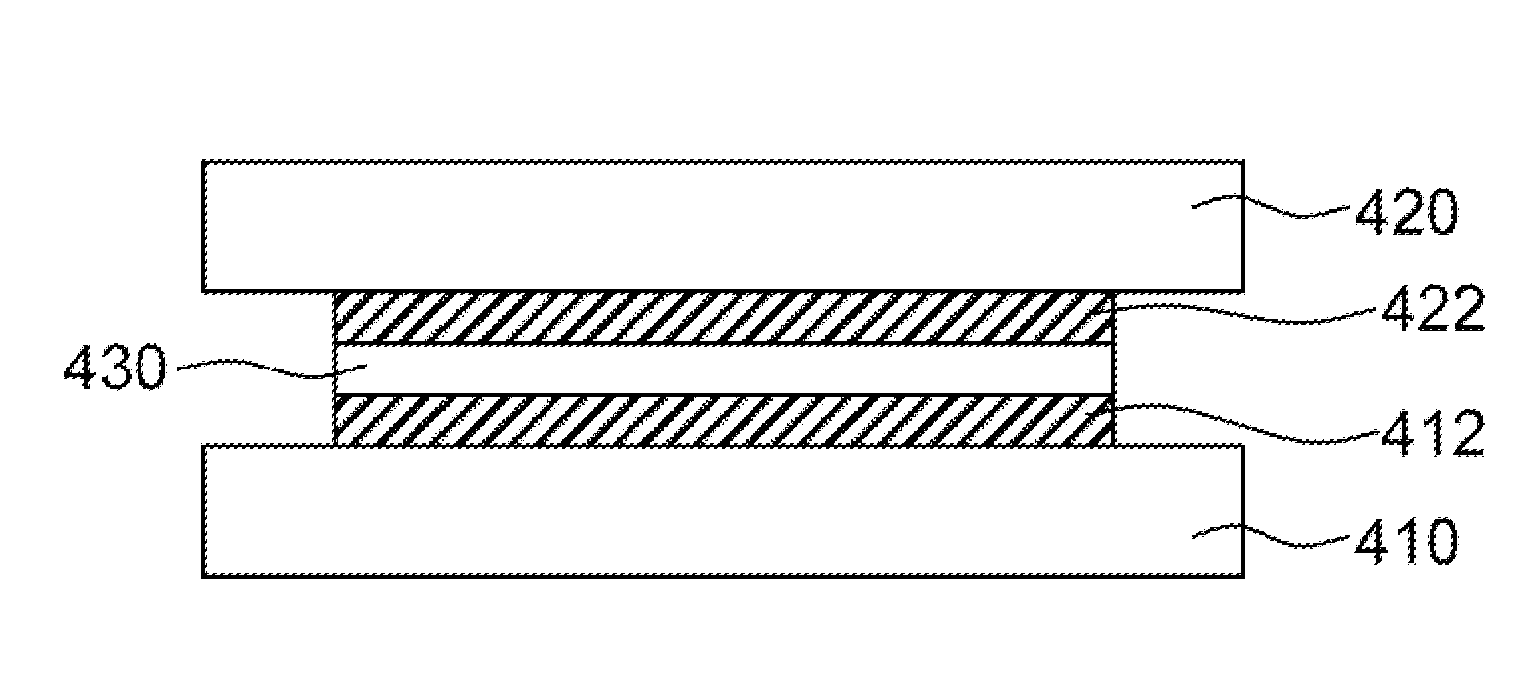
[0036]FIG. 4A is a cross-sectional view of a transparent capacitive touch panel according to a first embodiment of the present invention, and FIG. 4B is an exploded view of the transparent capacitive touch panel in FIG. 4A. Referring to FIG. 4A and FIG. 4B, the transparent capacitive touch panel 400 of the embodiment comprises a transparent substrate 410, a transparent cover lens 420 and a transparent adhesive layer 430. The first transparent electrode layer 422 and the second transparent electrode layer 412 are disposed respectively on the surfaces of the transparent cover lens 420 and the transparent substrate 412. A transparent adhesive layer 430 is used to bind the first transparent electrode layer 422 and the second transparent electrode layer 412 so as to combine the transparent substrate 410 and the transparent cover lens 420 that are disposed in parallel.

[0037]Compared to the prior art, in which two indium-tin oxide layers are formed on the surface of the transparent substra...

second embodiment

[0054]The first embodiment describes a single-layer structure, wherein the first transparent electrode layer and the second transparent electrode layer are respectively disposed on the surfaces of the transparent substrate and the transparent cover lens. In the present embodiment, the first transparent electrode layer and the second transparent electrode layer can both be manufactured on the surface of the transparent cover lens. Thereby, the transparent capacitive touch panel can do without the transparent substrate to further reduce the thickness of the transparent capacitive touch panel, as will be described hereinafter.

[0055]FIG. 8 is a cross-sectional view of a transparent capacitive touch panel according to a second embodiment of the present invention. Referring to FIG. 8, the transparent capacitive touch panel 800 in the present embodiment comprises a transparent cover lens 810, a first transparent electrode layer 812, an insulating layer 814 and a second transparent electrod...


PUM


Abstract

A transparent capacitive touch panel comprising a transparent substrate, a transparent cover lens and a transparent adhesive layer is provided, wherein a first transparent electrode layer and a second transparent electrode layer are disposed on the transparent cover lens and the transparent substrate respectively. The transparent adhesive layer is used to bind the first transparent electrode layer and second transparent electrode layer in order to combine the transparent cover lens and the transparent substrate disposed in parallel. Thereby, the manufacturing process of the transparent capacitive touch panel is simplified, and the manufacturing cost of the same is lowered.

Description

BACKGROUND OF THE INVENTION[0001]1. Field of the Invention[0002]The present invention generally relates to a touch panel and, more particularly to a transparent capacitive touch panel.[0003]2. Description of the Prior Art[0004]With the development in technologies, the electronic products having a touch panel as input such as personal digital assistants (PDA's), handsets, car navigating systems, tablet personal computers (PC's) have been widely used. The touch panel is provided on the screen for the user to use input information by a finger or a touch pen. There have been various kinds of touch panels developed. For example, the capacitive touch panel is based on the detection of the change of capacitance. Compared to the resistive touch panel based on direct touch, the capacitive touch panel exhibits higher transparency and longer lifetime.[0005]FIG. 1A is a cross-sectional view of a conventional transparent capacitive touch panel, and FIG. 1B is an exploded view of the transparent ...

Claims


Application Information

Patent Timeline
IPC IPC(8): G06F3/041G06F3/044
CPCG02F1/13338G06F3/044G06F3/0445G06F3/0412
Inventor WU, JASONHUNG, YEN-CHUNGWENG, RUEY-SHINGLAI, CHIH-CHANG
Owner TPK HLDG
Why Eureka
Try Eureka