Luminescence display and driving method thereof

a technology of oled display and driving method, which is applied in the direction of electroluminescent light sources, static indicating devices, instruments, etc., can solve the problems of increasing the cost of oled display, and achieve the effect of reducing the number of output lines

Active Publication Date: 2009-07-02
LG DISPLAY CO LTD
View PDF4 Cites 91 Cited by
  • Summary
  • Abstract
  • Description
  • Claims
  • Application Information

AI Technical Summary

Benefits of technology

[0008]An advantage of the present invention is to provide a luminescence display which is capable of reducing the number of output lines of a data driver, and a driving method thereof.
[0009]Additional features and advantages of the invention will be set forth in the description which follows, and in part will be apparent from the description, or may be learned by practice of the invention. The objectives and other advantages of the invention will be realized and attained by the structure particularly pointed out in the written description and claims hereof as well as the appended drawings.
[0010]To achieve these objects and other advantages and in accordance with the purpose of the invention, as embodied and broadly described, a OLED display includes: an OLED display panel including: data lines to which data voltages are supplied; gate lines to which a gate voltage is sequentially supplied; luminescence control lines to which a luminescence control voltage is sequentially supplied, a driving power line to which a driving voltage is supplied; a compensation power line to which a compensation voltage having a first level and a second level different from the first level are supplied; a plurality of pixel cells each respectively in pixel areas defined by the data lines and the gate lines; a data driver having output lines whose number is smaller than the number of the data lines; and a demultiplexer unit formed between the data driver and the OLED display panel, the demultiplexer unit supplying the data voltages from the output lines to the data lines, wherein each of the pixel cells includes: a light emitting element; and a pixel driver that supplies a current corresponding to a corresponding one of the data voltages to the light emitting element based on the corresponding data voltage, the gate voltage, the luminescence control voltage, the driving voltage and the compensation voltage having the first level and that turns off the light emitting element when the compensation voltage has the second level.
[0011]In another aspect of the present invention, a driving method for an OLED display, the OLED display including an OLED display panel having a plurality of pixel cells formed respectively in pixel areas defined by data lines to which data voltages are supplied, gate lines to which a gate voltage is sequentially supplied, luminescence control lines to which a luminescence control voltage is sequentially supplied, a driving power line to which a driving voltage is supplied, and a compensation power line to which compensation voltages of a first level and a second level different from the first level are supplied, the method including: supplying the data voltages from a data driver to the data lines through a demultiplexer unit between the data driver and the OLED display panel, the data driver having output lines whose number is smaller than the number of the data lines; sequentially supplying the gate voltage to the gate lines; supplying current corresponding to a corresponding one of the data voltages to a light emitting element of each of the pixel cells based on the luminescence control voltage, the driving voltage and the compensation voltage with the first level to turn on the light emitting element; and turning off the light emitting element based on the compensation voltage with the second level.
[0012]It is to be understood that both the foregoing general description and the following detailed description of the present invention are exemplary and explanatory and are intended to provide further explanation of the invention as claimed.

Problems solved by technology

As a result, the number of costly data driving integrated circuits (ICs) constituting the data driver not only increases, but processing time and manufacturing cost required for attaching the data driving ICs increases, which lead to an increase in the entire cost of the OLED display.

Method used


Image

  • Luminescence display and driving method thereof
  • Luminescence display and driving method thereof
  • Luminescence display and driving method thereof

Examples


first embodiment

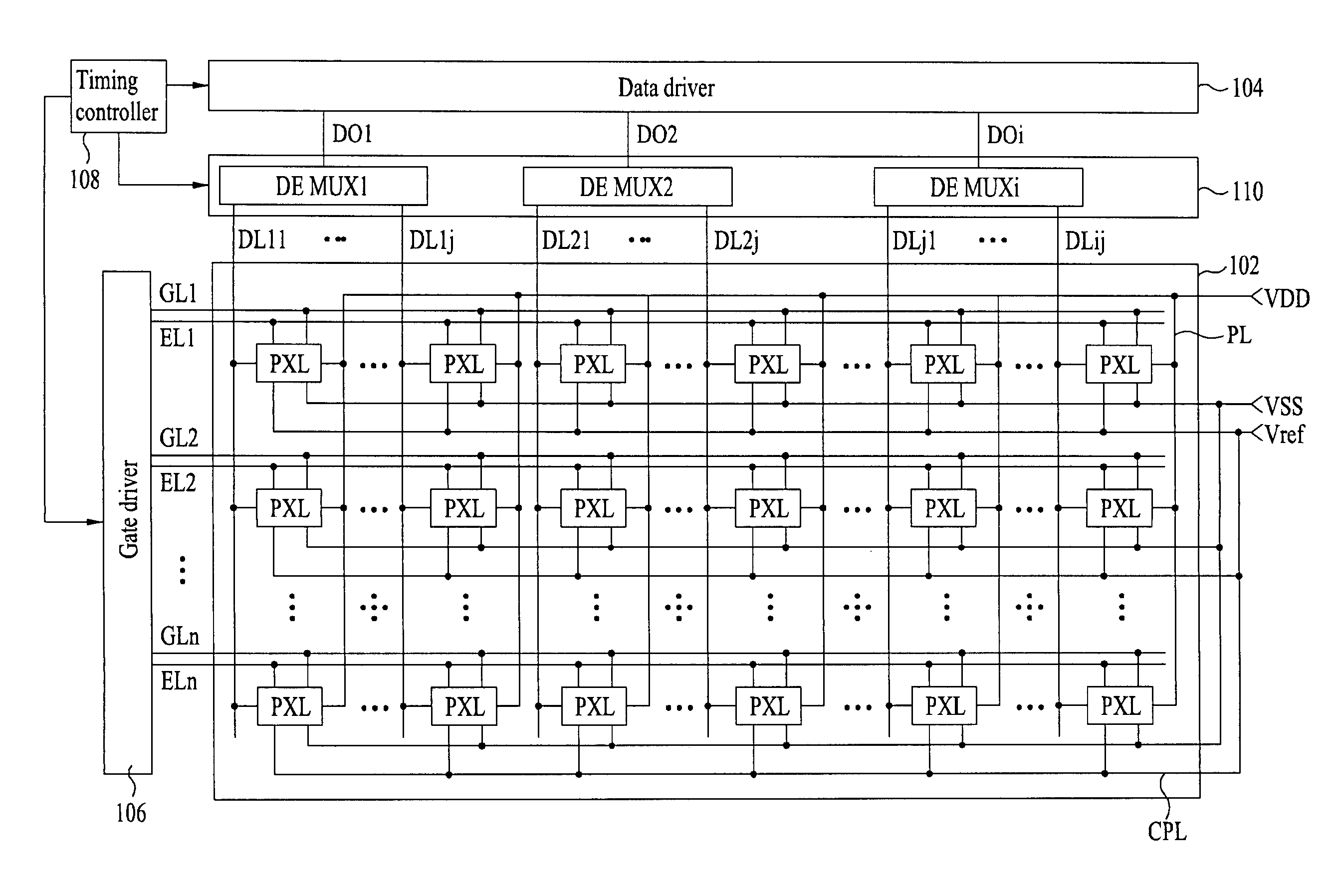
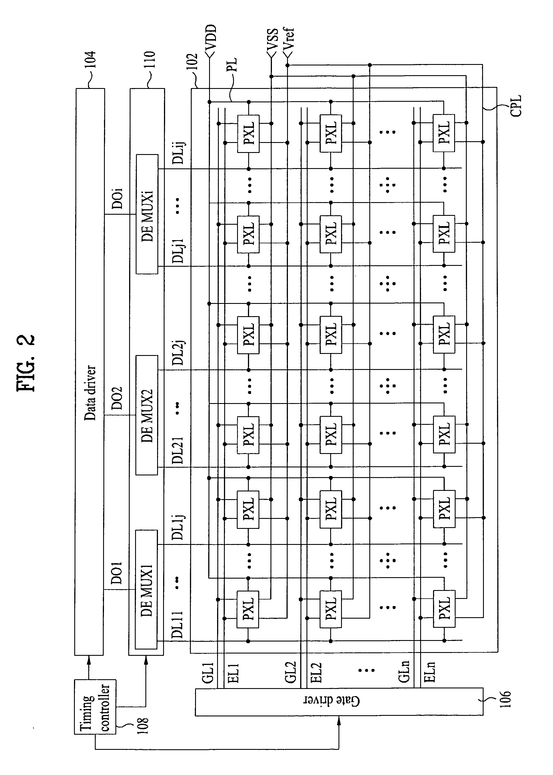
[0026]FIG. 2 is a block diagram showing the configuration of an OLED display according to the present invention.

[0027]Referring to FIG. 2, the OLED display according to the first embodiment of the present invention includes an OLED display panel 102, a gate driver 106 that drives gate lines GL1 to GLn of the OLED display panel 102, a data driver 104 that drives data lines DL11 to DLij of the OLED display panel 102, a demultiplexer unit 110 connecting the data driver 104 to the OLED display panel 102, and a timing controller 108 that controls the gate driver 106, data driver 104, and demultiplexer unit 110.

[0028]The OLED display panel 102 displays an image using a plurality of pixel cells PXL connected to the data lines DL, the gate lines GL, luminescence control lines EL, a driving power line PL, and a compensation power line CPL.

[0029]Each pixel cell PXL includes, as shown in FIG. 3, an OLED, and a pixel driver 112 for driving the OLED.

[0030]The pixel driver 112 includes first to f...

second embodiment

[0057]FIG. 8 is a circuit diagram of a pixel structure of an OLED display according to the present invention.

[0058]The pixel structure of the OLED display shown in FIG. 8 is the same as the pixel structure of the OLED display shown in FIG. 3, with the exception that it further includes a fifth switching transistor ST5 for supplying an initialization voltage Vini to the second node N2. Therefore, a detailed description of the same constituent elements will be omitted.

[0059]The fifth switching transistor ST5 supplies the initialization voltage Vini to the second node N2 in response to the low-logic gate voltage supplied to the gate line GLn-1 of the previous stage to initialize each pixel cell along a horizontal line. This fifth switching transistor ST5 has a gate terminal connected to the gate line GLn-1 of the previous stage, a source terminal connected to an initialization voltage Vini source, and a drain terminal connected to the second node N2. Here, the initialization voltage Vi...


PUM


Abstract

A OLED display and a driving method thereof are disclosed. The OLED display includes: an OLED display panel including: data lines to which data voltages are supplied; gate lines to which a gate voltage is sequentially supplied; luminescence control lines to which a luminescence control voltage is sequentially supplied, a driving power line to which a driving voltage is supplied; a compensation power line to which a compensation voltage having a first level and a second level different from the first level are supplied; a plurality of pixel cells each respectively in pixel areas defined by the data lines and the gate lines; a data driver having output lines whose number is smaller than the number of the data lines; and a demultiplexer unit formed between the data driver and the OLED display panel, the demultiplexer unit supplying the data voltages from the output lines to the data lines, wherein each of the pixel cells includes: a light emitting element; and a pixel driver that supplies a current corresponding to a corresponding one of the data voltages to the light emitting element based on the corresponding data voltage, the gate voltage, the luminescence control voltage, the driving voltage and the compensation voltage having the first level and that turns off the light emitting element when the compensation voltage has the second level.

Description

[0001]This application claims the benefit of the Korean Patent Application No. 2007-138359, filed on Dec. 27, 2007, which is hereby incorporated by reference for all purposes as if fully set forth herein.BACKGROUND OF THE INVENTION[0002]1. Field of the Invention[0003]The present invention relates to a luminescence display and a driving method thereof, and more particularly, to a luminescence display which is capable of reducing the number of output lines of a data driver, and a driving method thereof.[0004]2. Discussion of the Related Art[0005]An active matrix type organic electro-luminescence display (OLED) includes a plurality of pixel cells arranged in a matrix in order to display images. As shown in FIG. 1, each pixel cell 10 of the organic electro-luminescence display includes, an organic light emitting diode (OLED) and a pixel driver 12 for driving the OLED independently. The OLED has a cathode electrode connected to the pixel driver 12, an anode electrode connected to a power...

Claims


Application Information

Patent Timeline
Patent Type & Authority Applications(United States)
IPC IPC(8): G09G3/30
CPCG09G3/3233G09G3/3266G09G3/3291G09G2300/0819G09G2300/0861G09G2310/0262G09G2310/0297G09G2300/0842G09G3/20G09G3/30G09G3/32H05B33/12
Inventor JEON, CHANG HOONKIM, JUNG CHULLEE, HO YOUNG
Owner LG DISPLAY CO LTD
Why Eureka
Try Eureka