
Semiconductor memory device and method for operating the same

a memory device and semiconductor technology, applied in the field of semiconductor memory devices, can solve the problems that the basis for transferring operation commands and addresses cannot be aligned either, and the synchronous ddr semiconductor memory devices cannot meet the requirements of recent systems, and the high-speed semiconductor memory devices cannot operate normally

Active Publication Date: 2009-07-02
SK HYNIX INC
View PDF2 Cites 18 Cited by
  • Summary
  • Abstract
  • Description
  • Claims
  • Application Information

AI Technical Summary

Benefits of technology

[0026]Embodiments of the present invention are directed to providing a semiconductor memory device capable of performing a clock alignment training without delay factors affected by variations of process, voltage, and temperature (PVT) to output an internal data always at a predetermined timing regardless of the PVT variations, and a method for operating the semiconductor memory device.

Problems solved by technology

However, even the DDR synchronous semiconductor memory device cannot meet the requirement of recent systems for inputting / outputting mass amounts of data at high speed.
However, if the phases of the system clock and the data clock are not aligned, then the basis for transferring an operation command and an address and the basis for transferring data cannot be aligned either.
This also means that the high-speed semiconductor memory device cannot operate normally.

Method used


Image

  • Semiconductor memory device and method for operating the same
  • Semiconductor memory device and method for operating the same
  • Semiconductor memory device and method for operating the same

Examples


first embodiment

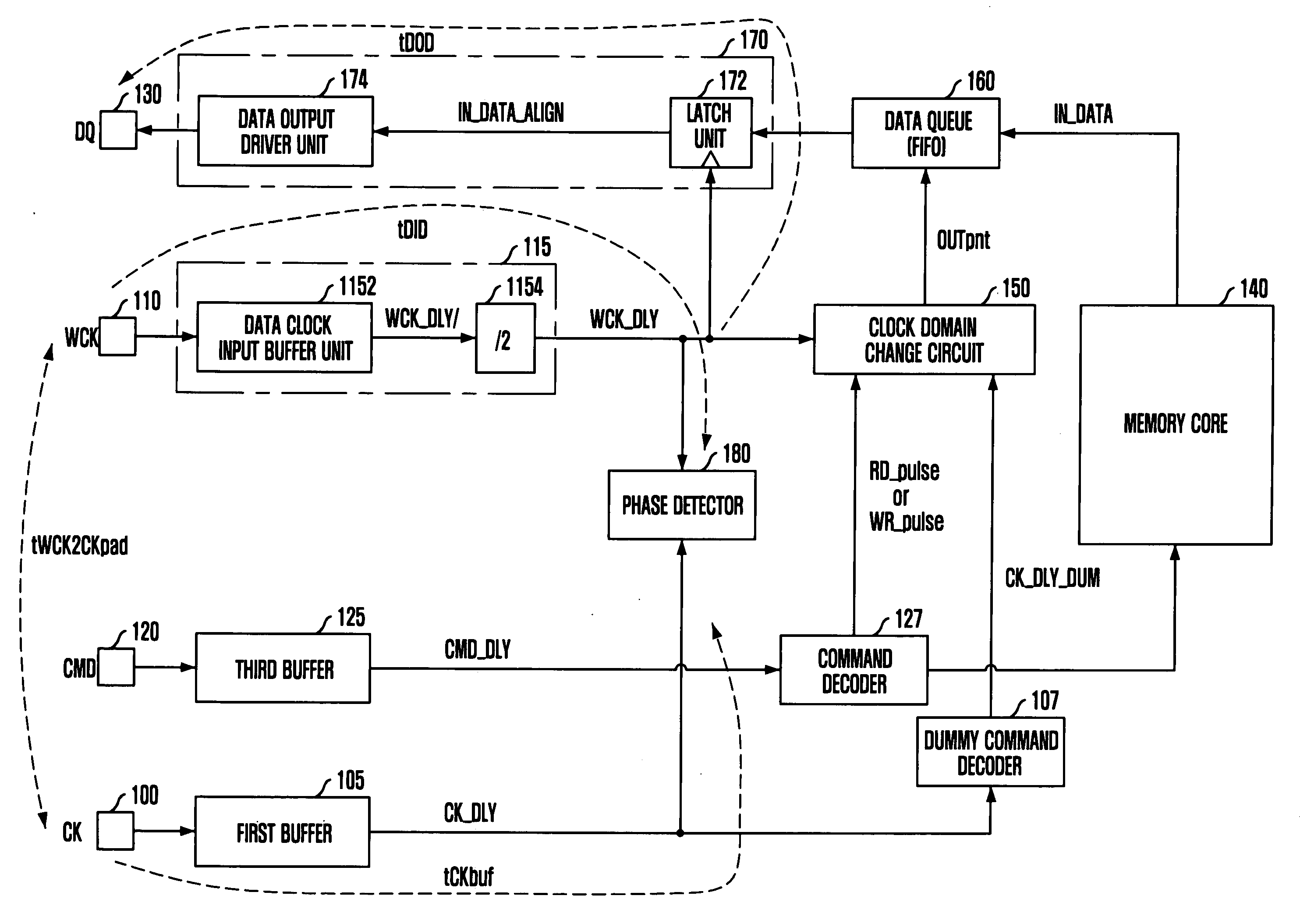
[0038]FIG. 1 is a block diagram of a semiconductor memory device in accordance with the present invention.

[0039]Referring to FIG. 1, the semiconductor memory device includes a first pad 100, a second pad 110, a third pad 120, a first buffer 105, a second buffer 115, a third buffer 125, a phase detector 180, a memory core 140, a clock domain change circuit 150, a data queue 160, and a data output circuit 170. The semiconductor memory device further includes a command decoder 127, and a dummy command decoder 107. The first pad 100 receives a system clock CK from an external controller to synchronize an address signal and an operation command CMD to the system clock CK. The second pad 110 receives a data clock WCK of a higher frequency than the system clock CK from the external controller to synchronize a data signal to the data clock WCK. The third pad 120 receives the operation command CMD. The first buffer 105 buffers the system clock CK input from the first pad 100. The second buff...

second embodiment

[0057]FIG. 3 is a block diagram of a semiconductor memory device in accordance with the present invention.

[0058]Referring to FIG. 3, the semiconductor memory device includes a first pad 300, a second pad 310, a third pad 320, a first buffer 305, a second buffer 315, a third buffer 325, a memory core 340, a clock domain change circuit 350, a data queue 360, a data output circuit 370, a phase detector 380, and a compensation delay unit 390. The semiconductor memory device further includes a command decoder 327, and a dummy command decoder 307. The first pad 300 receives a system clock CK from an external controller to synchronize an address signal and an operation command CMD to the system clock CK. The second pad 310 receives a data clock WCK of a higher frequency than the system clock CK from the external controller to synchronize a data signal to the data clock WCK. The third pad 320 receives the operation command CMD. The first buffer 305 buffers the system clock CK input from the...


PUM


Abstract

A semiconductor memory device includes a first buffering unit configured to buffer a first clock for an address signal and a command to be input in synchronization with the first clock, a second buffering unit configured to buffer a second clock for a data signal to be in synchronization with the second clock to output a buffered second clock having the same frequency as the first clock, a data output circuit configured to output an internal data in response to the buffered second clock, a delay unit configured to delay the buffered second clock by a predetermined time, and a phase detector configured to detect a phase difference of an output clock of the delay unit and the output clock of the first buffering unit, and to output the detection result.

Description

CROSS-REFERENCE(S) TO RELATED APPLICATIONS[0001]The present invention claims priority of Korean patent application number 10-2007-0138019, filed on Dec. 26, 2007, which is incorporated by reference in its entirety.BACKGROUND OF THE INVENTION[0002]The present invention relates to a semiconductor device, and more particularly to a semiconductor memory device capable of performing a clock alignment training especially to output internal data at a predetermined timing regardless of variations of process, voltage, and temperature (PVT), and a method for operating the semiconductor memory device.[0003]In a system with a variety of semiconductor devices, a semiconductor memory device serves as a data storage. The semiconductor memory device outputs data corresponding to addresses received from a data processor, e.g., a memory control unit (MCU), or stores data received from the data processor into memory cells selected by the addresses.[0004]As the operating speed of the system is increasi...

Claims


Application Information

Patent Timeline
Patent Type & Authority Applications(United States)
IPC IPC(8): G11C7/00G11C8/18
CPCG11C7/1051G11C7/1066G11C7/1078G11C2207/2254G11C7/22G11C7/222G11C8/18G11C7/1093G11C11/4093G11C11/4096G11C11/4076G11C11/407
Inventor KIM, KYUNG-HOONYOON, SANG-SIC
Owner SK HYNIX INC
Learn More