Pixel driving circuit and a display device having the same

a driving circuit and display device technology, applied in the direction of electric digital data processing, instruments, computing, etc., can solve the problems of losing the benefit of boosting voltage and insufficient mounting space, so as to reduce and increase the voltage level of the driving control signal

Active Publication Date: 2009-07-09
SAMSUNG DISPLAY CO LTD
View PDF4 Cites 19 Cited by
  • Summary
  • Abstract
  • Description
  • Claims
  • Application Information

AI Technical Summary

Benefits of technology

[0028]In accordance with an exemplary embodiment of the present invention, a pixel driving circuit includes: an input unit, a first signal output unit, and a second signal output unit. The input unit is configured to output a driving control signal according to a (Pn−2)th stage driving signal output from the (Pn−2)th previous stage unit and a (Pn+2)th stage driving signal output from the (Pn+2)th stage unit. The first signal output unit is configured to output a stage driving signal according to the driving control signal and a driving clock signal and to change the voltage level of the driving control signal. The second signal output unit is configured to output a gate voltage signal to the corresponding gate line according to the driving control signal and a gate clock signal and to change the voltage level of the driving control signal.
[0029]The gate line may be connected to at least one of a plurality of pixels. The pixel driving circuit may further include a boosting voltage provider configured to provide a boosting voltage to the pixels connected to the corresponding gate line according to the driving control signal after the gate voltage signal of a high logic level is provided to the corresponding gate line.
[0030]In accordance with an exemplary embodiment of the present invention, a method of driving a pixel driving circuit includes: generating a logic-high driving control signal according to one of a (Pn−2)th stage driving signal and a (Pn+2)th stage driving signal; applying a logic-high driving clock signal to generate a logic-high stage driving signal and to increase the voltage level of the driving control signal; applying a logic-high gate clock signal to apply a logic-high gate voltage signal to a corresponding gate line and to increase the voltage level of the driving control signal; applying a logic-low gate clock signal to apply a logic-low gate voltage signal to the corresponding gate line and to reduce the voltage level of the driving control signal; applying a logic-low driving clock signal to generate a logic-low stage driving signal and to reduce the voltage level of the driving control signal; and generating a logic-low driving control signal according to the other of the (Pn−2)th stage driving signal and the (Pn+2)th stage driving signal.
[0031]The method may further include providing a boosting voltage to a plurality of pixels connected to the gate line after the applying of the logic-low gate voltage signal to the corresponding gate line.
[0032]The driving control signal may maintain a logic-high level for four periods (4H). The logic-high gate voltage signal may be applied to the corresponding gate line for at least one of three periods (3H) of the four periods (4H), except the last period of the four periods (4H). The boosting voltage may be provided for the last period.

Problems solved by technology

However, a sufficient mounting space is needed to mount the gate driver.
However, when the display panel is then rotated by 180°, the boosting voltage is provided before application of the gate turn-on voltage, thus losing the benefit of the boosting voltage.

Method used


Image

  • Pixel driving circuit and a display device having the same
  • Pixel driving circuit and a display device having the same
  • Pixel driving circuit and a display device having the same

Examples


Embodiment Construction

[0044]Hereinafter, exemplary embodiments of the present invention will be described in further detail with reference to the accompanying drawings.

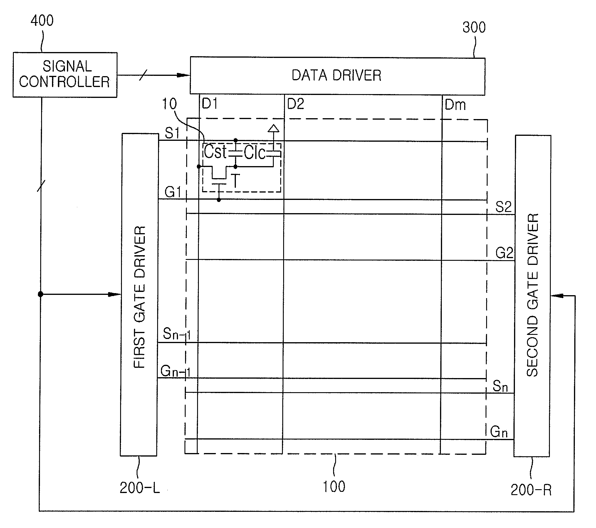
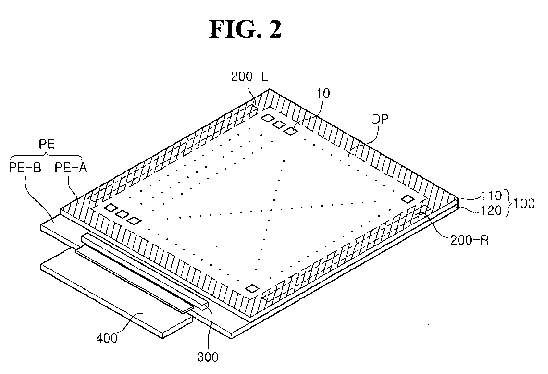
[0045]FIG. 1 is a block diagram of a display device according to an exemplary embodiment of the present invention. FIG. 2 is a perspective view of the display device according to an exemplary embodiment of the present invention. FIG. 3 is a block diagram of first and second gate drivers according to an exemplary embodiment of the present invention. FIG. 4 is a circuit diagram of a stage unit according to an exemplary embodiment of the present invention.

[0046]Referring to FIGS. 1 through 4, a display device includes a display panel 100, first and second gate drivers 200-L and 200-R, a data driver 300, and a signal controller 400.

[0047]As illustrated in FIG. 1, the display panel 100 includes a plurality of gate lines G1 through Gn extending in one direction, and a plurality of data lines D1 through Dm extending in a direction intersecting th...


PUM


Abstract

A pixel driving circuit includes a first driver and a second driver. The first gate driver includes a plurality of stage units connected to odd-numbered gate lines. The second gate driver includes a plurality of stage units connected to even-numbered gate lines. Each of the stage units of the first and second gate drivers includes an input unit, a first signal output unit, and a second signal output unit. The input unit outputs a driving control signal according to a previous stage driving signal output from the previous stage unit and a next stage driving signal output from the next stage unit. The first signal output unit outputs a stage driving signal according to the driving control signal and a driving clock signal. The second signal output unit outputs a gate voltage signal to the corresponding gate line according to the driving control signal and a gate clock signal.

Description

CROSS-REFERENCE TO RELATED APPLICATION[0001]This application claims priority to Korean Patent Application No. 10-2008-0001398, filed on Jan. 4, 2008, under 35 U.S.C. §119, the contents of which are incorporated by reference in their entirety herein.BACKGROUND[0002]1. Technical Field[0003]The present disclosure relates to a pixel driving circuit and a display device having the same, and more particularly, to a pixel driving circuit and a display device having the same, with a varying scan direction.[0004]2. Discussion of Related Art[0005]Display devices can display an image by providing image signals to a plurality of pixels. A liquid crystal display (LCD) device displays a desired image by changing the light transmittance of liquid crystal for each pixel. Such a display device includes: a display panel having a plurality of pixels; and gate / data drivers controlling the operations of the pixels. The gate driver provides a gate turn-on voltage (e.g., a scan signal) sequentially to a p...

Claims


Application Information

Patent Timeline
Patent Type & Authority Applications(United States)
IPC IPC(8): G09G5/00
CPCG09G3/3648G09G3/3677G09G2300/0426G09G2310/0224G09G2340/0492G09G2310/0283G09G2320/0261G09G2320/028G09G2310/0267G02F1/133G09G3/20G09G3/36
Inventor PARK, SANG-JINCHA, YOUNG-OKLEE, JOO-HYUNG
Owner SAMSUNG DISPLAY CO LTD
Why Eureka
Try Eureka