
Optical plate, display device having the optical plate, and method of manufacturing the optical plate

a technology of optical plate and display device, which is applied in the field of optical plate, can solve the problems of deteriorating requiring additional processes to manufacture the optical plate, and so as to improve the stability of the dimension complicating the manufacture of the optical plate, and increasing the manufacturing cost of the optical plate

Inactive Publication Date: 2009-07-16
SAMSUNG DISPLAY CO LTD
View PDF0 Cites 8 Cited by
  • Summary
  • Abstract
  • Description
  • Claims
  • Application Information

AI Technical Summary

Benefits of technology

[0007]Since the manufacturing or forming of prism patterns on an optical plate may include heat and / or pressure, the optical plate may be deformed due to the heat and / or pressure. For example, the heat and / or pressure deforming the optical plate may thereby deteriorate the stability of dimension of the optical plate. Furthermore, since the optical plate may be deformed, additional processes may be required to manufacture the optical plate. For example, post-treatment such as cutting may be required to complete the manufacturing of the optical plate, thereby complicating the manufacture of the optical plate and increasing the manufacturing cost of the optical plate.
[0008]An exemplary embodiment provides an optical plate which contributes to the stability of dimension of the optical plate during manufacturing and the reduction of manufacturing costs.
[0009]An exemplary embodiment provides a display device including an optical plate which contributes to the stability of dimension and the reduction of manufacturing costs.
[0010]An exemplary embodiment provides a method of manufacturing an optical plate which contributes to the stability of dimension and the reduction of manufacturing costs.

Problems solved by technology

For example, the heat and / or pressure deforming the optical plate may thereby deteriorate the stability of dimension of the optical plate.
Furthermore, since the optical plate may be deformed, additional processes may be required to manufacture the optical plate.
For example, post-treatment such as cutting may be required to complete the manufacturing of the optical plate, thereby complicating the manufacture of the optical plate and increasing the manufacturing cost of the optical plate.

Method used


Image

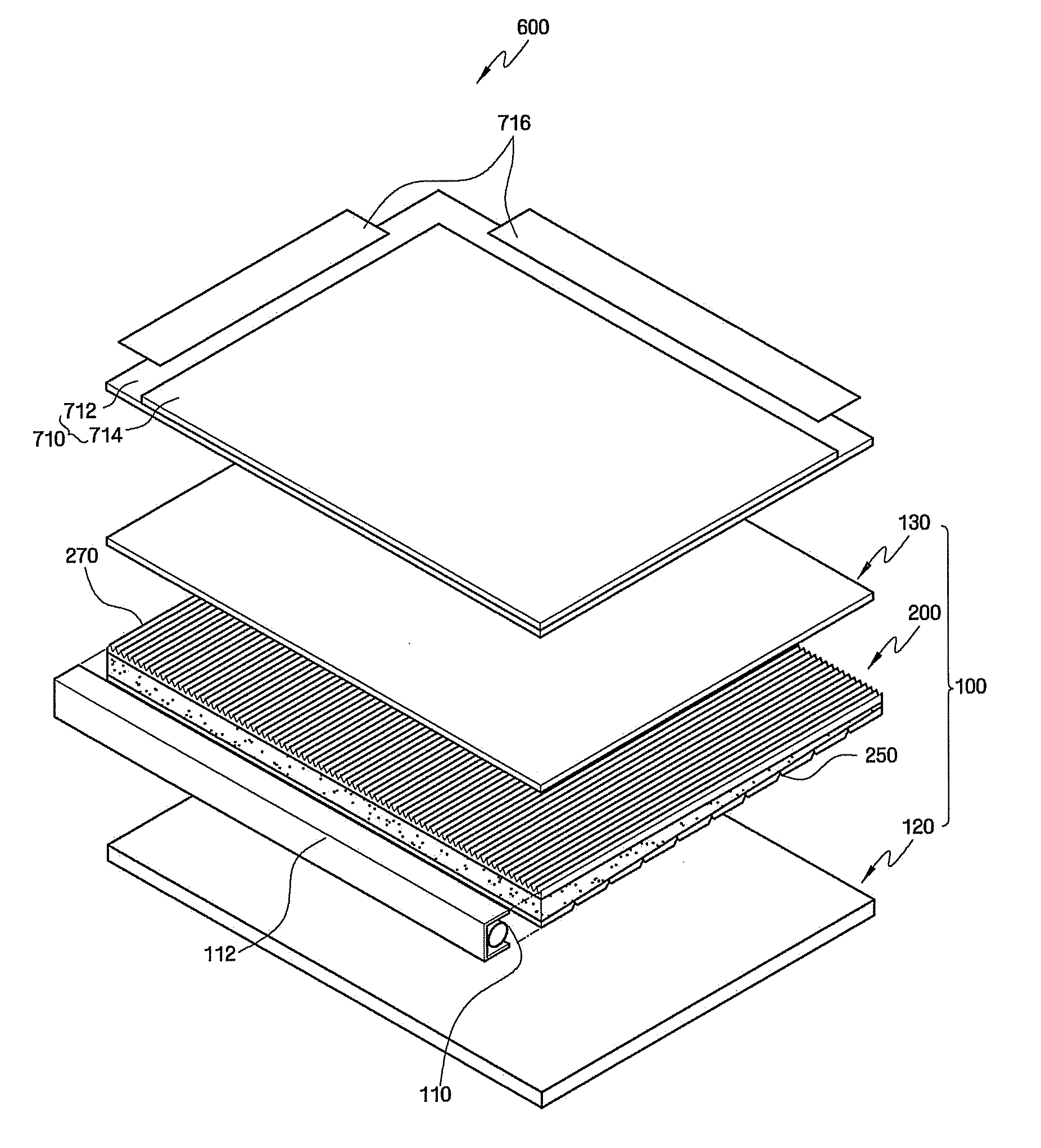
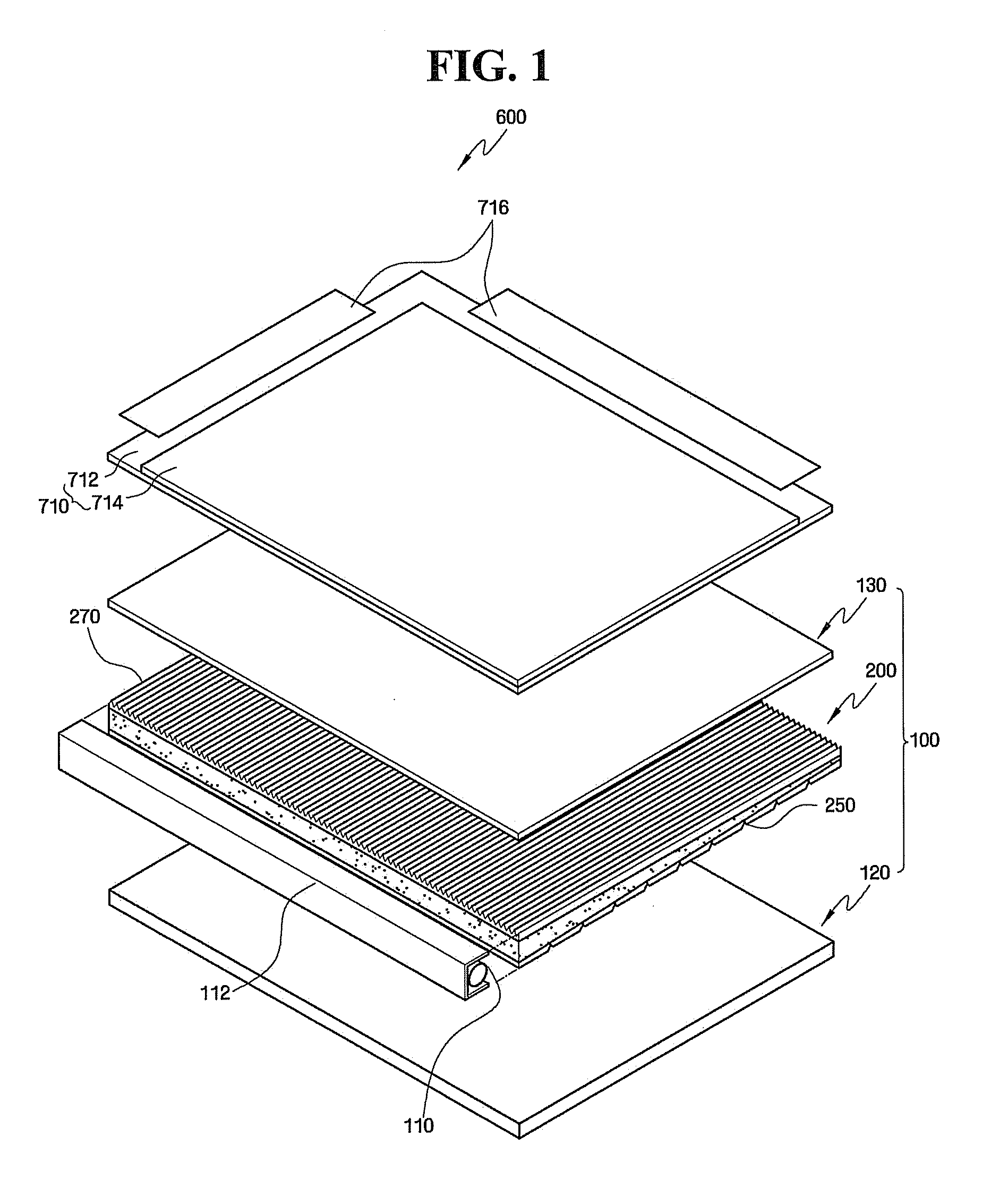
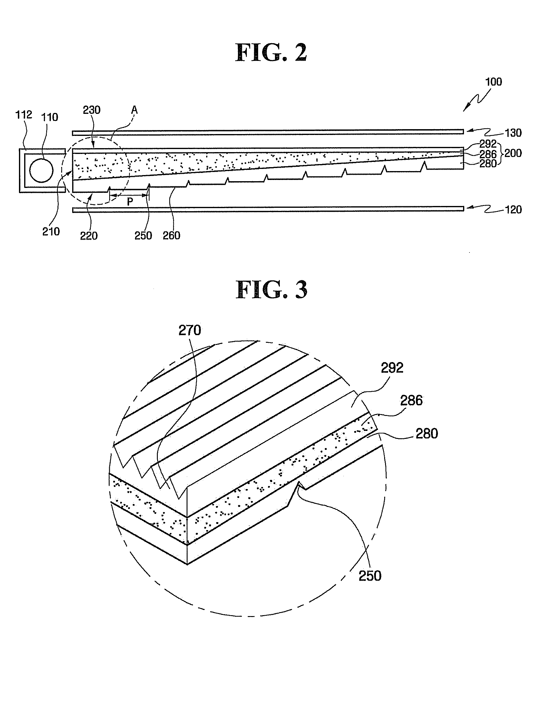
  • Optical plate, display device having the optical plate, and method of manufacturing the optical plate
  • Optical plate, display device having the optical plate, and method of manufacturing the optical plate
  • Optical plate, display device having the optical plate, and method of manufacturing the optical plate

Examples


Embodiment Construction

[0030]The present invention will now be described more fully with reference to the accompanying drawings, in which exemplary embodiments of the invention are shown. The invention may, however, be embodied in many different forms and should not be construed as being limited to the embodiments set forth herein. Rather, these embodiments are provided so that this disclosure will be thorough and complete, and will fully convey the concept of the invention to those skilled in the art.

[0031]It will be understood that when an element is referred to as being “connected to” or “disposed on” another element, it can be directly connected to or disposed on the other element or intervening elements may be present. In contrast, when an element is referred to as being “directly connected to” or “directly disposed on” another element, there are no intervening elements present. Like numbers refer to like elements throughout. As used herein the term “and / or” includes any and all combinations of one o...


PUM

PropertyMeasurementUnit
transmittanceaaaaaaaaaa
glass transition temperatureaaaaaaaaaa

Abstract

An optical plate includes a core layer and a surface layer. The surface layer is disposed on at least one surface of the core layer and includes a plurality of prism patterns. The core layer and the surface layer have different glass transition temperatures.

Description

[0001]This application claims priority to Korean Patent Application No. 10-2008-0005071 filed on Jan. 16, 2008, and all the benefits accruing therefrom under 35 U.S.C. §119, the disclosure of which is incorporated herein by reference in its entirety.BACKGROUND OF THE INVENTION[0002]1. Field of the Invention[0003]The present invention relates to an optical plate, a display device having the optical plate and a method of manufacturing the optical plate, and more particularly, to an optical plate contributing to the stability of dimension and the reduction of manufacturing costs, a display device having the optical plate and a method of manufacturing the optical plate.[0004]2. Description of the Related Art[0005]A liquid crystal display (“LCD”) may include two display panels having a plurality of electrodes, such as pixel electrodes and common electrodes, generating an electric field, and a liquid crystal layer interposed between the two display panels. An LCD controls the polarization...

Claims


Application Information

Patent Timeline
Patent Type & Authority Applications(United States)
IPC IPC(8): G02F1/13357F21V5/02B29D11/00G02B1/04
CPCB29D11/00278G02B6/0038G02F2202/08G02F1/133606G02F2001/133607G02B6/0046G02F1/133607G02B5/04G02B6/00
Inventor SONG, MIN-YOUNGCHOI, JIN-SUNGJOO, BYUNG-YUNLEE, SANG-HOONKIM, DONG-KWAN
Owner SAMSUNG DISPLAY CO LTD
Learn More