Method for manufacturing a CMOS device having dual metal gate

Active Publication Date: 2009-07-16
UNITED MICROELECTRONICS CORP
View PDF14 Cites 36 Cited by
  • Summary
  • Abstract
  • Description
  • Claims
  • Application Information

AI Technical Summary

Benefits of technology

[0011]According to the method for manufacturing a CMOS device having dual metal gate, at least a conductive type transistor is formed by the gate last process, therefore the method is more applicable to form the conductive type transistor needed to avoid high heat budget. Thus Vfb roll-off issue is improved and material choice for the metal gate is widened. In addition, since the high-K gate dielectric layer is not

Problems solved by technology

With a trend towards scaling town the CMOS size, conventional methods, which are used to achieve optimization, such as reducing thickness of the gate dielectric layer, for example the thickness of silicon dioxide layer, have faced problems such as leakage current due to tunneling effect.
On the other hand, the conventional polysilicon gate also has faced problems such as inferior performance due to bor

Method used


Image

  • Method for manufacturing a CMOS device having dual metal gate
  • Method for manufacturing a CMOS device having dual metal gate
  • Method for manufacturing a CMOS device having dual metal gate

Examples


Embodiment Construction

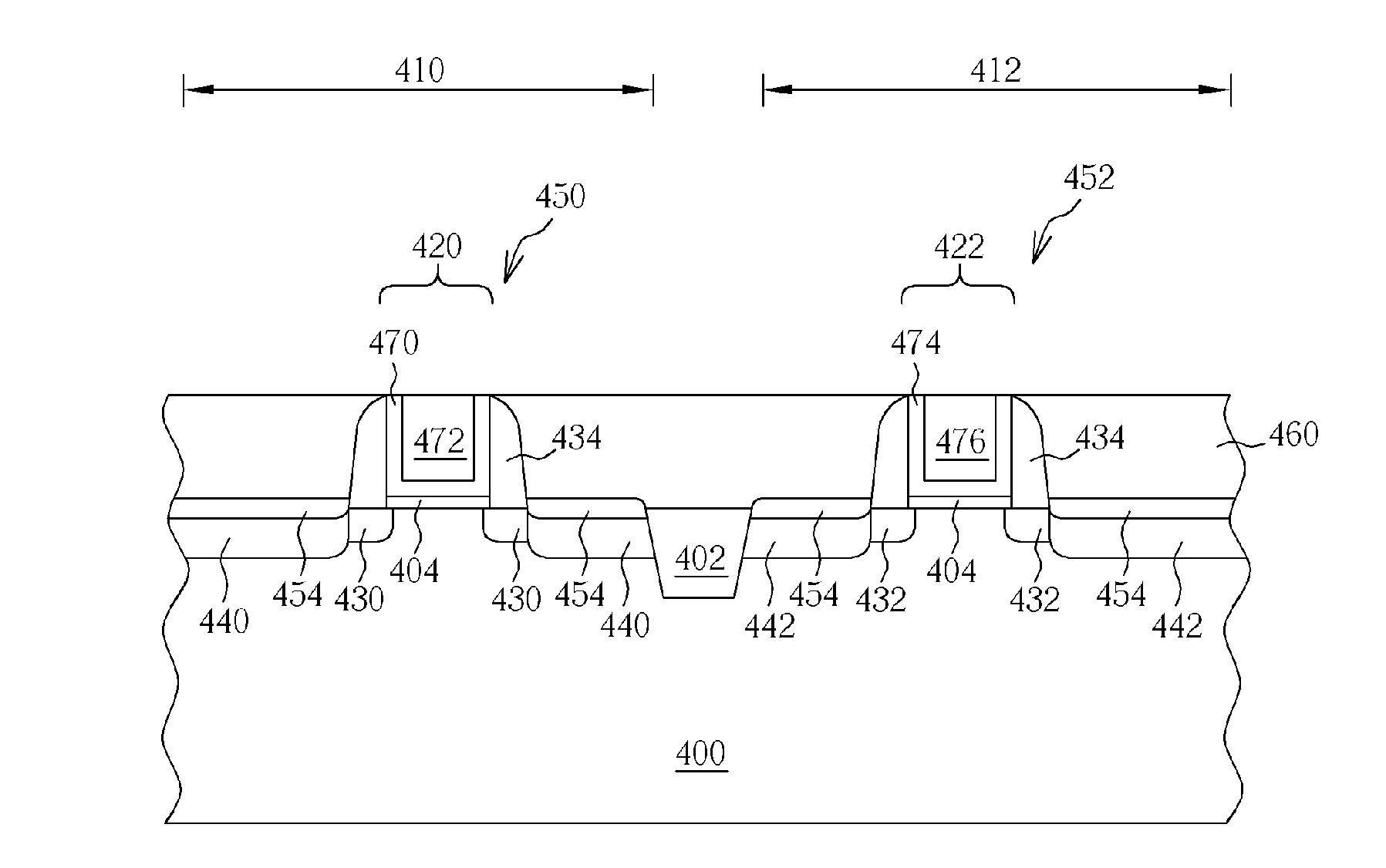
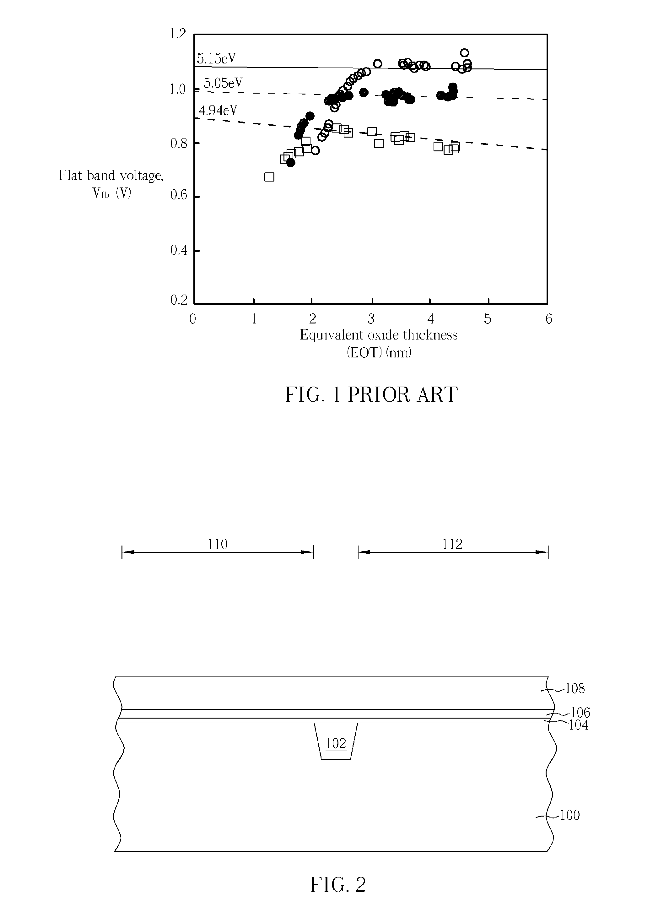
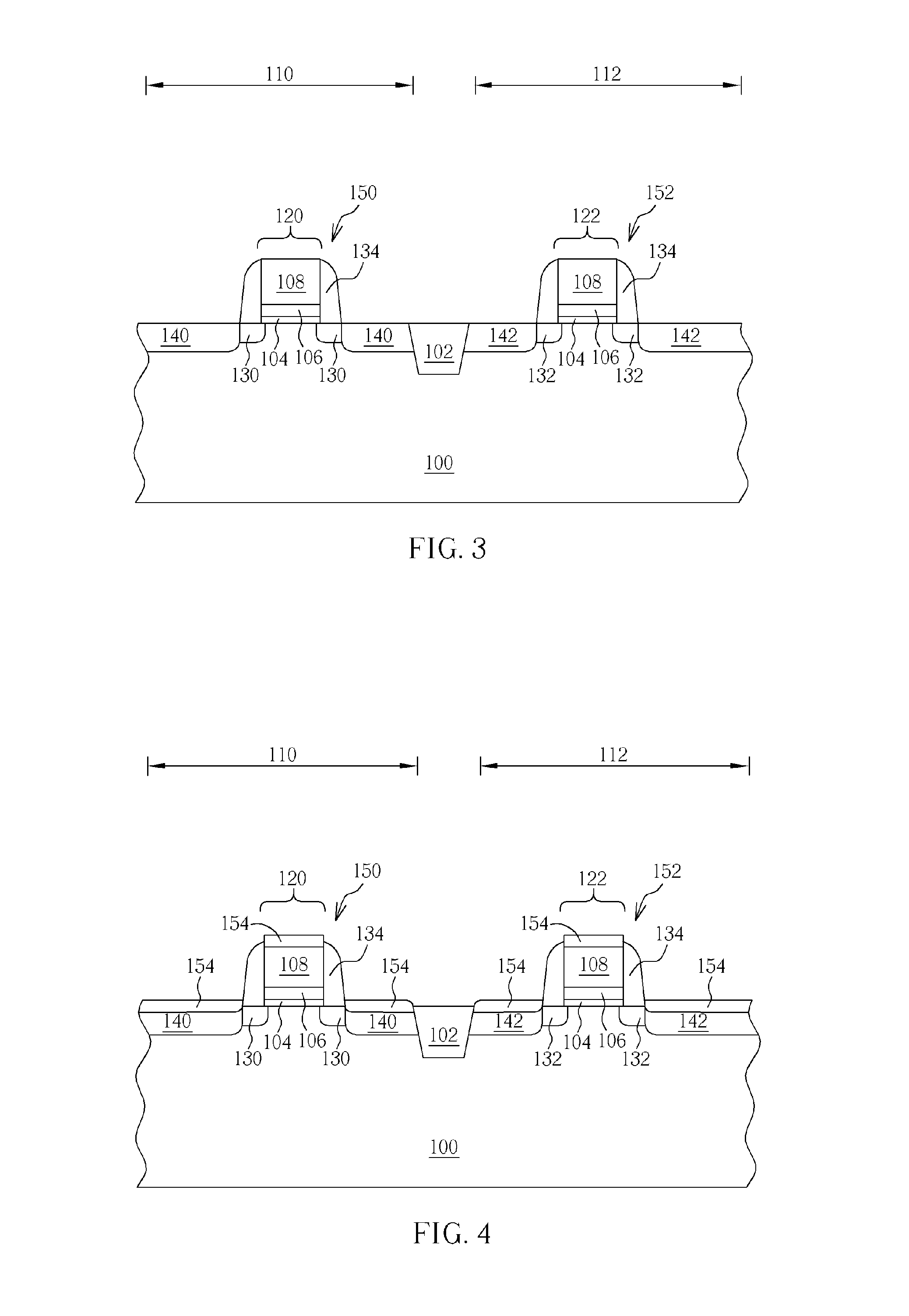
[0018]Please refer to FIGS. 2-8, which are schematic drawings illustrating a method for manufacturing a CMOS device having dual metal gate according to a first preferred embodiment of the present invention. As shown in FIG. 2, a substrate 100, such as a silicon substrate, a silicon-containing substrate, or a silicon-on-insulator (SOI) substrate, having a first active region 110 and a second active region 112 defined thereon is provided. The substrate 100 comprises a shallow trench isolation (STI) 102 used to provide electrical isolation between the first active region 110 and the second active region 112. Then, a high-K gate dielectric layer 104, a TaC layer 106, and a polysilicon layer 108 are sequentially formed on the substrate 100. Furthermore, a protective layer not shown) can be formed in between the high-K gate dielectric layer 104 and the TaC layer 106 for protecting the high-K gate dielectric layer 104 from damage during the following processes in the first preferred embodi...


PUM


Abstract

A method for manufacturing a CMOS device includes providing a substrate having a first active region and a second active region defined thereon, forming a first conductive type transistor and a second conductive type transistor respectively in the first and the second active regions, performing a salicide process, forming an ILD layer, performing a first etching process to remove a first gate of the first conductive type transistor and to form an opening while a high-K gate dielectric layer is exposed in a bottom of the opening, and forming at least a first metal layer in the opening.

Description

BACKGROUND OF THE INVENTION[0001]1. Field of the Invention[0002]The invention relates to a method for manufacturing a complementary metal-oxide semiconductor (CMOS) device having a dual metal gate, and more particularly, to a method for manufacturing a CMOS device with a gate last process.[0003]2. Description of the Prior Art[0004]With a trend towards scaling town the CMOS size, conventional methods, which are used to achieve optimization, such as reducing thickness of the gate dielectric layer, for example the thickness of silicon dioxide layer, have faced problems such as leakage current due to tunneling effect. In order to keep progression to next generation, high-K materials are used to replace the conventional silicon oxide to be the gate dielectric layer because it decreases physical limit thickness effectively, reduces leakage current, and obtains equivalent capacitor in an identical equivalent oxide thickness (EOT).[0005]On the other hand, the conventional polysilicon gate a...

Claims


Application Information

Patent Timeline
IPC IPC(8): H01L21/8238
CPCH01L21/823807H01L21/823842H01L29/495H01L29/7843H01L29/517H01L29/665H01L29/66545H01L29/4966
Inventor LIN, CHIEN-TINGCHENG, LI-WEIHSU, CHE-HUAMA, GUANG-HWAYANG, CHIN-SHENG
Owner UNITED MICROELECTRONICS CORP
Why Eureka
Try Eureka