Method for manufacturing a CMOS device having dual metal gate

a technology of complementary metaloxide and metal gate, which is applied in the direction of semiconductor devices, basic electric elements, electrical appliances, etc., can solve the problems of leakage current, the thickness of the gate dielectric layer, and the conventional methods used to achieve optimization, so as to avoid high heat budget and widen the material choice of metal gates

Active Publication Date: 2009-07-23
UNITED MICROELECTRONICS CORP
View PDF6 Cites 78 Cited by
  • Summary
  • Abstract
  • Description
  • Claims
  • Application Information

AI Technical Summary

Benefits of technology

[0010]According to the method for manufacturing a CMOS device having dual metal gate provided by the present invention, the transistors are fabricated with the gate last process. Since high-temperature processes have already finished before constructing the metal gates of the transistors, the provided method is more applicable to form the transistor needed to avoid high heat budget. Accordingly Vfb roll-off issue is improved and material choice for the metal gate is widened.

Problems solved by technology

With a trend towards scaling down the CMOS size, conventional methods used to achieve optimization, such as reducing thickness of the gate dielectric layer, for example the thickness of silicon dioxide layer, have faced problems such as leakage current due to tunneling effect.
On the other hand, the conventional polysilicon gate also has faced problems such as inferior performance due to boron penetration and unavoidable depletion effect which increases equivalent thickness of the gate dielectric layer, reduces gate capacitance, and worsens a driving force of the devices.
Instead, a roll-off issue is observed.

Method used


Image

  • Method for manufacturing a CMOS device having dual metal gate
  • Method for manufacturing a CMOS device having dual metal gate
  • Method for manufacturing a CMOS device having dual metal gate

Examples


Embodiment Construction

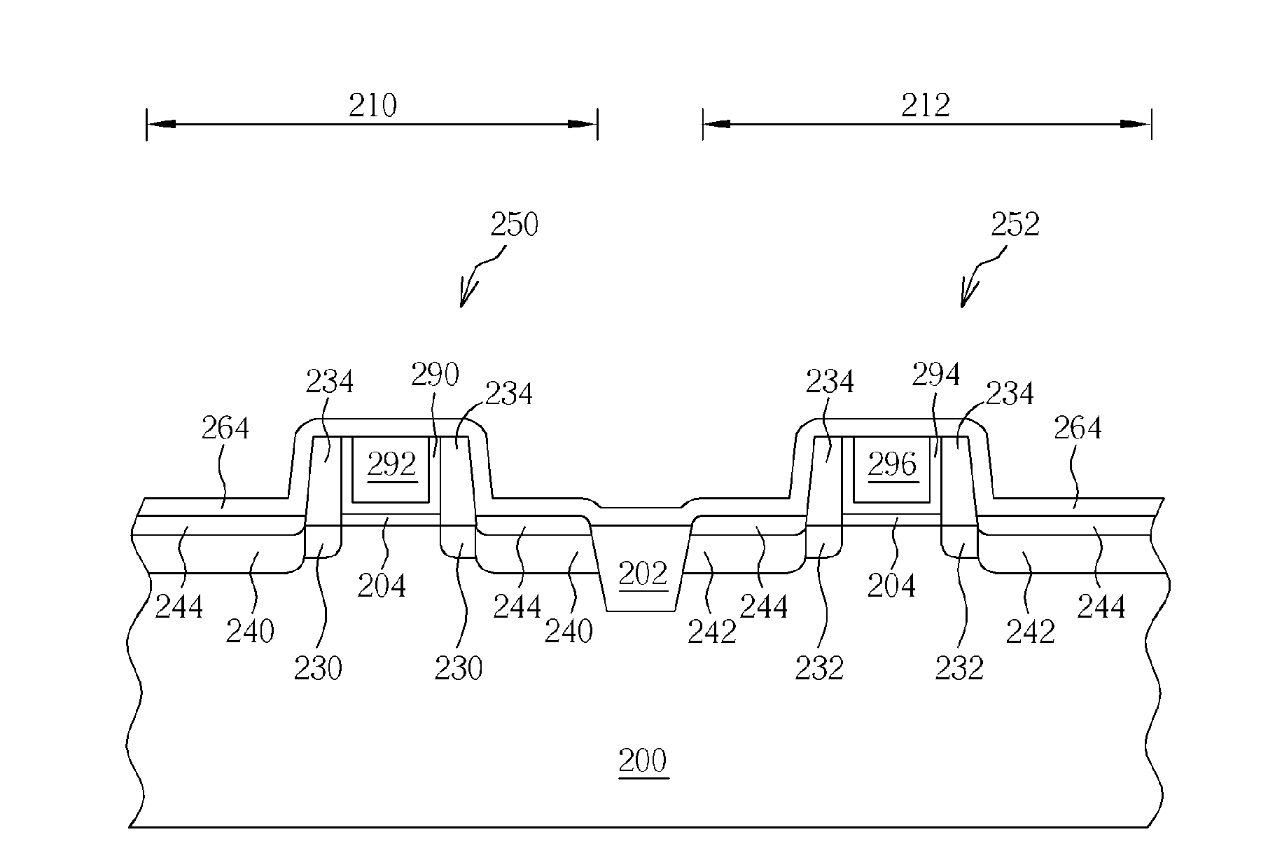
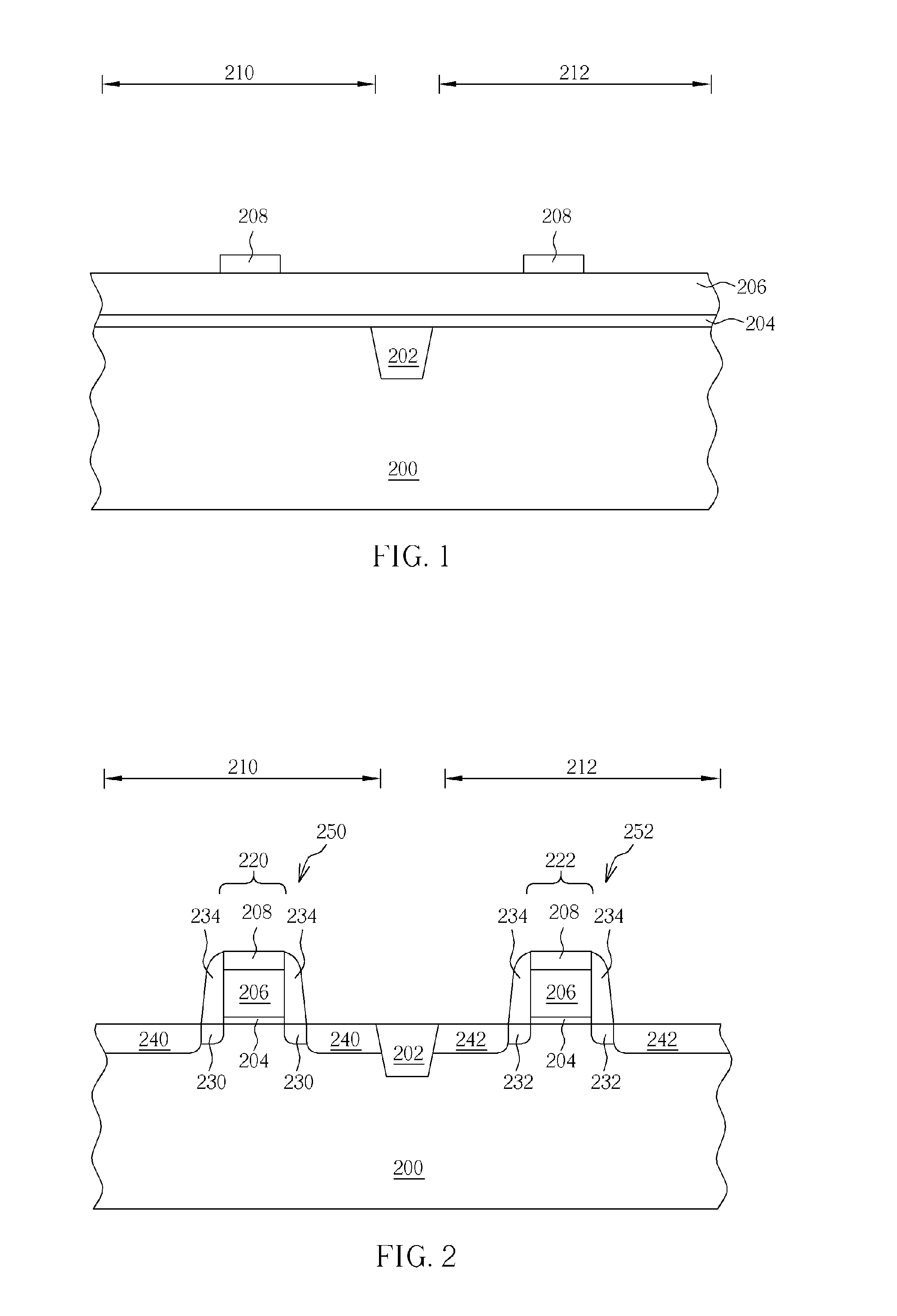
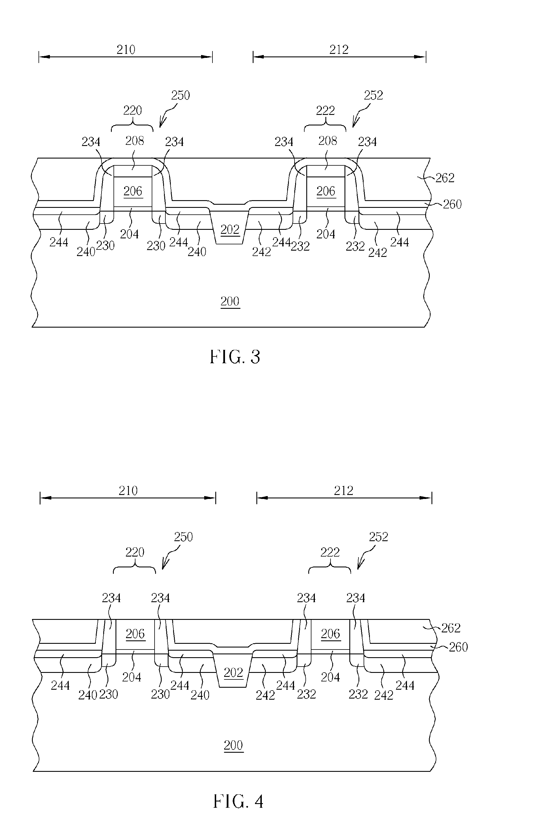
[0013]Please refer to FIGS. 1-13, which are schematic drawings illustrating a method for manufacturing a CMOS device having dual metal gate according to a preferred embodiment of the present invention. As shown in FIG. 1, a substrate 200 such as a silicon substrate, a silicon-containing substrate, or a silicon-on-insulator (SOI) substrate, having a first active region 210 and a second active region 212 defined thereon is provided. The substrate 200 further comprises a shallow trench isolation (STI) 202 used to provide an electrical isolation between the first active region 210 and the second active region 212. Then, a gate dielectric layer 204, a gate conductive layer such as a polysilicon layer 206, a hard mask layer (not shown) are sequentially formed on the substrate 200. The gate dielectric layer 204 can be a silicon oxide layer or a silicon oxynitride layer; it also can be a high-K dielectric layer. In addition, a cap layer (not shown) or an ARC layer (not shown) can be selecti...


PUM


Abstract

A method for manufacturing a CMOS device having dual metal gate includes providing a substrate having at least two transistors of different conductive types and a dielectric layer covering the two transistors, planarizing the dielectric layer to expose gate conductive layers of the two transistors, forming a patterned blocking layer exposing one of the conductive type transistor, performing a first etching process to remove a portion of a gate of the conductive type transistor, reforming a metal gate, removing the patterned blocking layer, performing a second etching process to remove a portion of a gate of the other conductive type transistor, and reforming a metal gate.

Description

BACKGROUND OF THE INVENTION[0001]1. Field of the Invention[0002]The invention relates to a method for manufacturing a complementary metal-oxide semiconductor (CMOS) device having a dual metal gate, and more particularly, to a method for manufacturing a CMOS device applied with a gate last process.[0003]2. Description of the Prior Art[0004]With a trend towards scaling down the CMOS size, conventional methods used to achieve optimization, such as reducing thickness of the gate dielectric layer, for example the thickness of silicon dioxide layer, have faced problems such as leakage current due to tunneling effect. In order to keep progression to next generation, high-K materials are used to replace the conventional silicon oxide to be the gate dielectric layer because it decreases physical limit thickness effectively, reduces leakage current, and obtains equivalent capacitor in an identical equivalent oxide thickness (EOT).[0005]On the other hand, the conventional polysilicon gate also...

Claims


Application Information

Patent Timeline
Patent Type & Authority Applications(United States)
IPC IPC(8): H01L21/28
CPCH01L21/823807H01L21/823842H01L29/7843H01L29/66545H01L29/7833H01L29/4966
Inventor YU, CHIH-HAOCHENG, LI-WEICHIANG, TIAN-FUCHOU, CHENG-HSIENLIN, CHIEN-TINGHSU, CHE-HUAMA, GUANG-HWA
Owner UNITED MICROELECTRONICS CORP
Why Eureka
Try Eureka