Resistor and manufacturing method thereof

Active Publication Date: 2013-02-28
UNITED MICROELECTRONICS CORP
View PDF2 Cites 24 Cited by
  • Summary
  • Abstract
  • Description
  • Claims
  • Application Information

AI Technical Summary

Benefits of technology

The present invention provides a method for making a resistor integrated with a transistor with metal gate. The method simplifies the manufacturing process and improves the material selection and process window. Additionally, the metal portions in the resistor improve its stability and performance.

Problems solved by technology

In the current semiconductor field, though the fabricating processes are improved with the aim of reaching high yields, it is found that integration of the manufacturing methods of those different kinds of semiconductor devices are very complicated and difficult.

Method used


Image

  • Resistor and manufacturing method thereof
  • Resistor and manufacturing method thereof
  • Resistor and manufacturing method thereof

Examples


Embodiment Construction

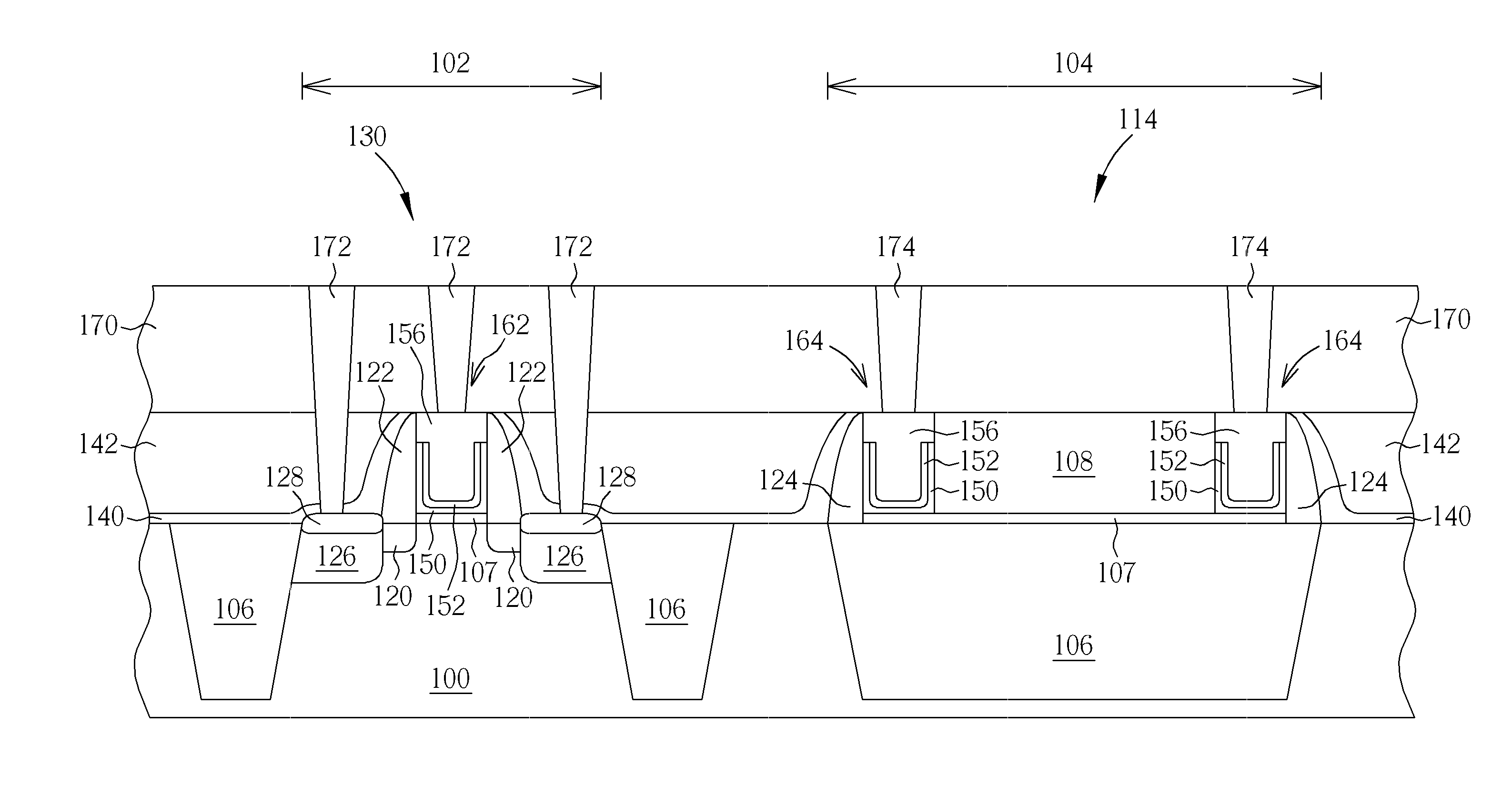
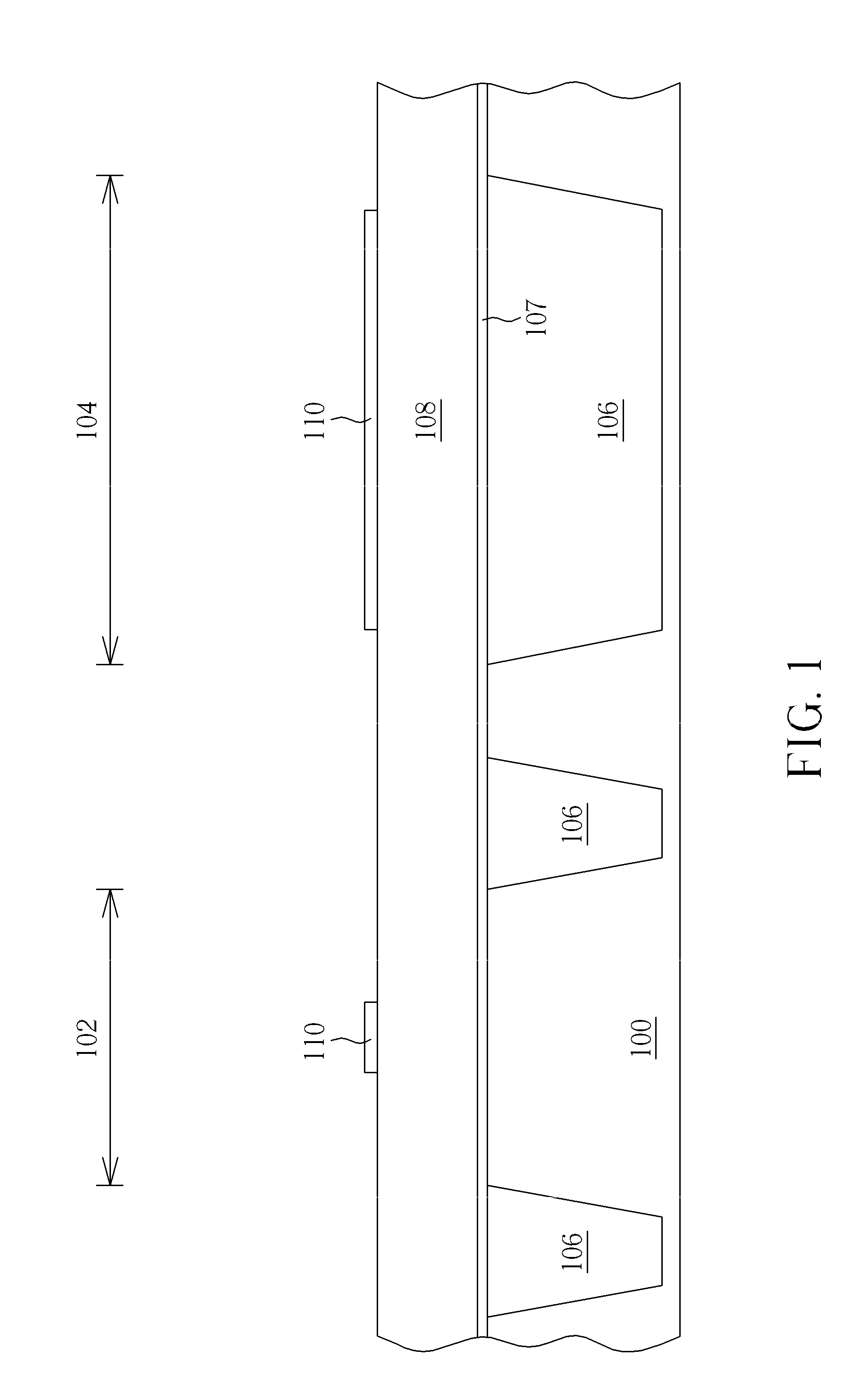
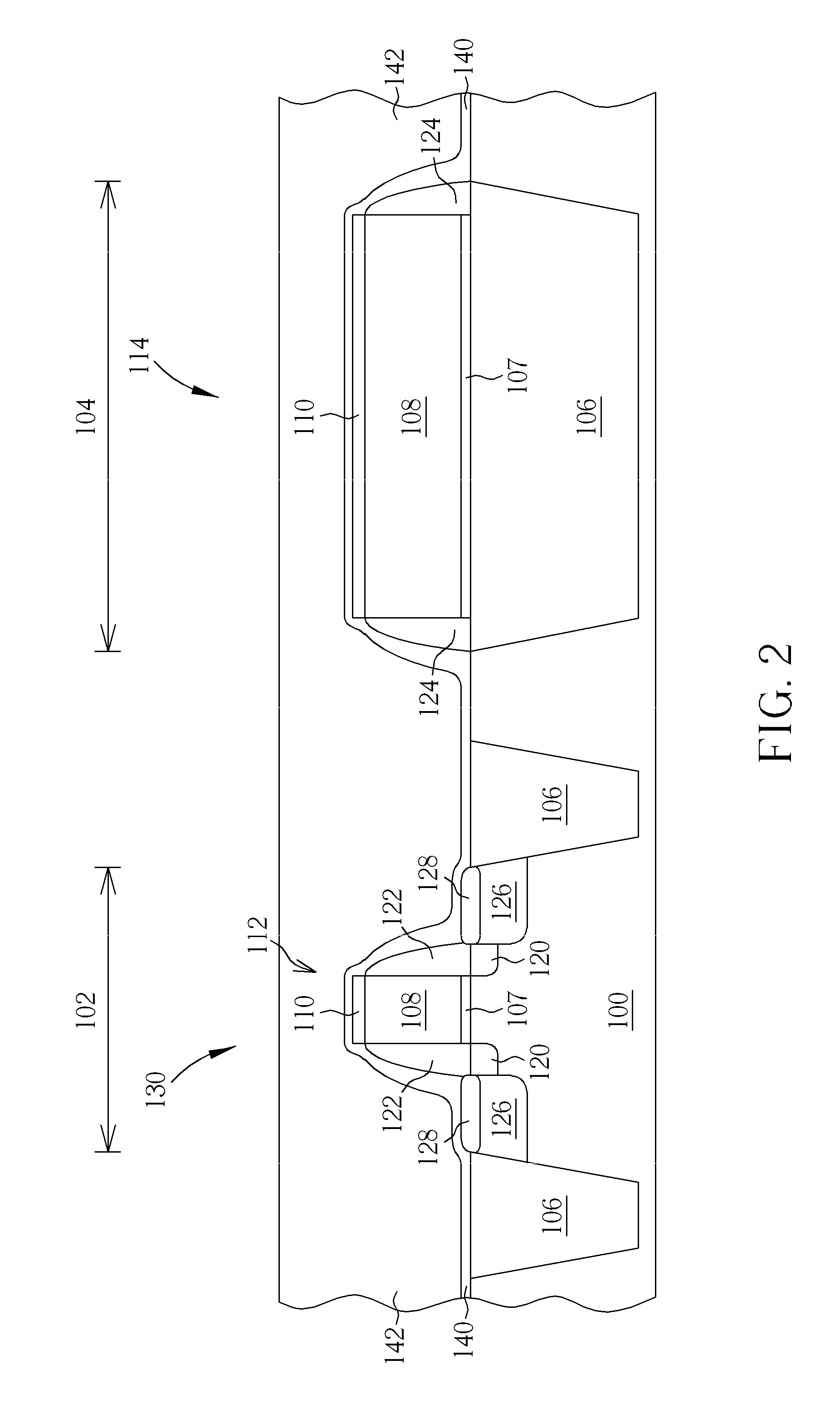
[0019]Please refer to FIGS. 1-8, which are schematic drawings illustrating a manufacturing method for a resistor integrated with a transistor having metal gate provided by a preferred embodiment of the present invention. As shown in FIG. 1, a substrate 100 having a transistor region 102 and a resistor region 104 defined thereon is provided. The substrate 100 also includes a plurality of shallow trench isolations (STIs) 106 positioned in between devices for providing electrical isolation. It is noteworthy that a STI 106 is formed in the resistor region 104. Then, a dielectric layer 107, a polysilicon layer 108, and a patterned hard mask 110 are sequentially formed on the substrate 100. The patterned hard mask 110 is formed to define a gate for a transistor and a resistor. It is noteworthy that the dielectric layer 107 formed between the substrate 100 and the polysilicon layer 108 can include conventional dielectric material such as silicon oxide.

[0020]Please refer to FIG. 2. Next, an...


PUM


Abstract

A manufacturing method for a resistor integrated with a transistor having metal gate includes providing a substrate having a transistor region and a resistor region defined thereon, respectively forming a transistor having a dummy gate in the transistor region and a resistor in the resistor region, removing the dummy gate and portions of the resistor to form a first trench in the transistor and two second trenches in the resistor, forming at least a high-k gate dielectric layer in the first trench and the second trenches, and forming a metal gate in the first trench and metal structures respectively in the second trenches.

Description

BACKGROUND OF THE INVENTION[0001]1. Field of the Invention[0002]The invention relates to a resistor and a manufacturing method thereof, and more particularly, to a resistor and a manufacturing method for a resistor integrated with a transistor having metal gate.[0003]2. Description of the Prior Art[0004]To increase the performance of transistors, metal gates are popularly used in the semiconductor field: the metal gates competent to the high dielectric constant (hereinafter abbreviated as high-K) gate dielectric layer replace the traditional polysilicon gates to be the control electrode. The metal gate approach can be categorized to the gate first process and the gate last process. And the gate last process gradually replaces the gate first process because it provides more material choices for the high-k gate dielectric layer and the metal gate.[0005]Additionally, resistors are elements which are often used for providing regulated voltage and for filtering noise in a circuit. The re...

Claims


Application Information

Patent Timeline
IPC IPC(8): H01C7/00H01L21/02
CPCH01L28/20H01L29/66545H01L27/0629
Inventor YANG, JIE-NINGHSU, SHIH-CHIEHLIN, CHUN-HSIENWANG, YAO-CHANGPAI, CHI-HORNTSENG, CHI-SHENG
Owner UNITED MICROELECTRONICS CORP
Why Eureka
Try Eureka