Single-Wafer Etching Method for Wafer and Etching Apparatus Thereof

a single-wafer etching and etching technology, applied in the direction of basic electric elements, electrical equipment, semiconductor/solid-state device manufacturing, etc., can solve problems such as microscopic etching unevenness

Inactive Publication Date: 2009-07-16
SUMCO CORP
View PDF10 Cites 13 Cited by
  • Summary
  • Abstract
  • Description
  • Claims
  • Application Information

AI Technical Summary

Benefits of technology

[0013]It is an object of the present invention to provide a single-wafer etching method for a wafer that can uniformly etch an edge portion without collapsing a chamfered shape of the edge portion of the wafer and can prevent a glitter from being produced on an edge surface of the wafer, and an etching apparatus thereof.
[0014]As a result of keenly examining the above-explained problems, the present inventors have discovered that adjusting a gap between a lower surface blow mechanism that blows off an etchant toward a radially outer side of a wafer and a wafer rear surface to a very limited predetermined range enables uniformly etching an edge portion without collapsing a chamfered shape of the edge portion of the wafer and also enables assuredly preventing a glitter from being produced on an edge surface, thereby bringing the present invention to completion.

Problems solved by technology

Although a reason that the gap GP strongly affects production of the glitter is unknown, it can be considered that, since the wafer 11 is rotating, the gas flowing through the gap GP becomes a turbulence flow when the gap GP is wide, and the etchant 14 flows to the edge surface on the rear surface side of the wafer 11 even though it is a small amount, resulting in microscopic etching unevenness.

Method used


Image

  • Single-Wafer Etching Method for Wafer and Etching Apparatus Thereof
  • Single-Wafer Etching Method for Wafer and Etching Apparatus Thereof
  • Single-Wafer Etching Method for Wafer and Etching Apparatus Thereof

Examples


example 1

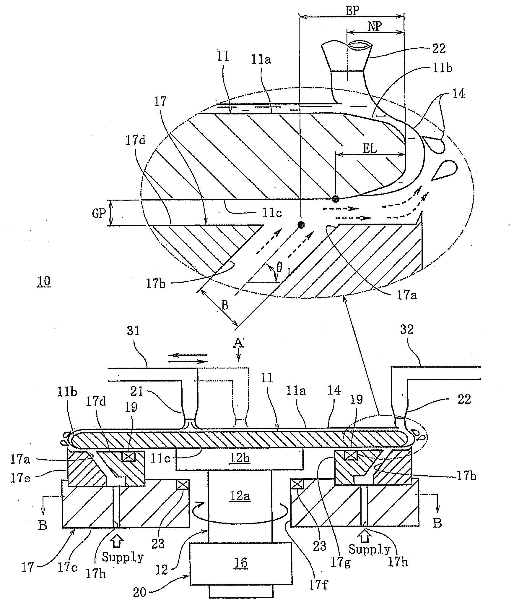
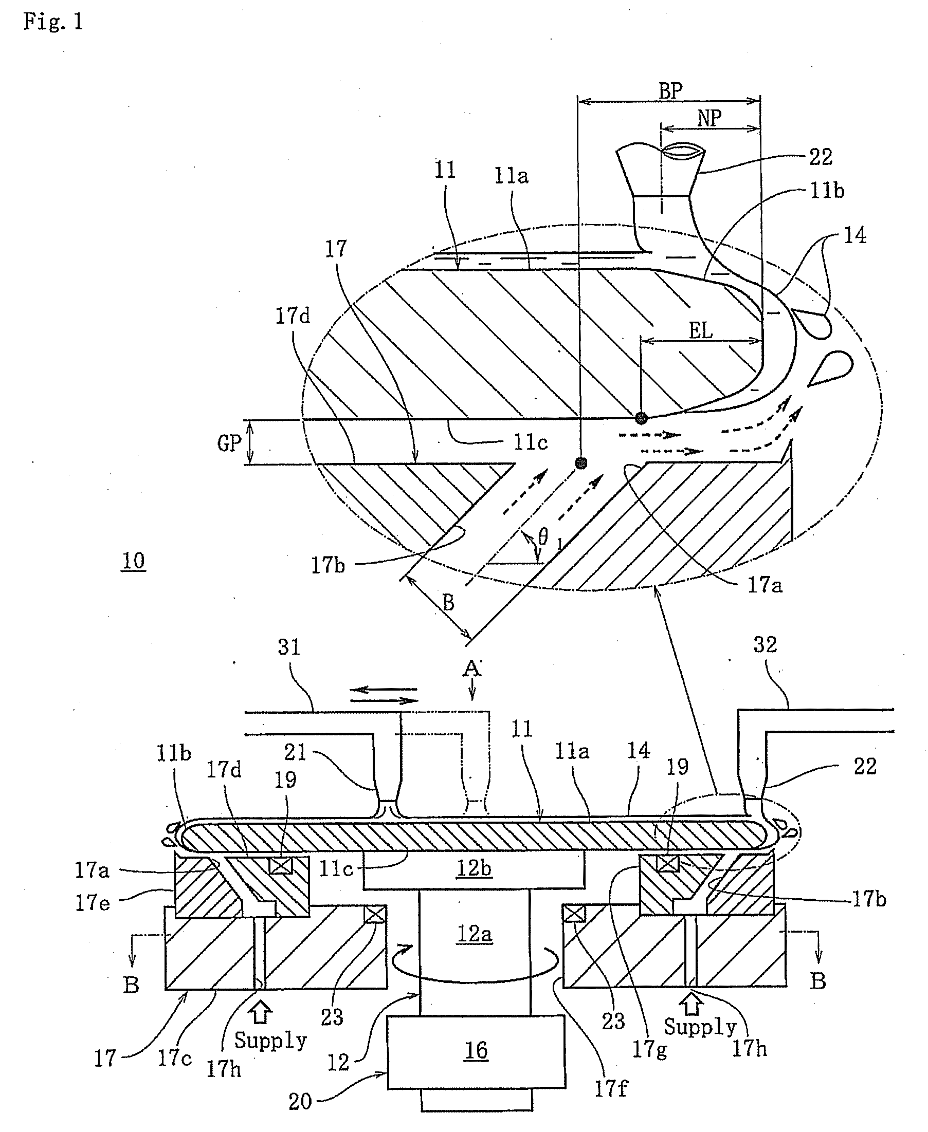
[0054]As shown in FIG. 1, the single-wafer etching apparatus 10 was used to etch the silicon wafer 11 having a diameter of 300 mm and a thickness of 0.8 mm. Here, the gap adjusting means 20 adjusted the gap GP between the upper surface of the lower surface blow mechanism 17 and the lower surface 11c of the wafer 11 to 0.4 mm, and the position BP of the injection tip 17a was set to a position that is 3 mm from the wafer outer rim toward the radially inner side of the wafer. Furthermore, the flow volume BF of the gas injected from the injection tip 17a was set to 500 liters / minute, and G / B was set to 500 where G liters / minute is a flow volume of the gas from the injection tip 17a and B mm is a width of the injection tip. Moreover, the rotating speed of the wafer 11 was set to 400 rpm, the angle θ1 of the injection groove 17b with respect to the horizontal plane was set to 30 degrees, the flow volume of the etchant 14 emitted from the first nozzle 21 was set to 3 liters / minute, the fir...


PUM

PropertyMeasurementUnit
angleaaaaaaaaaa
angleaaaaaaaaaa
angle θ1aaaaaaaaaa

Abstract

A single-wafer etching apparatus according to the present invention supplies an etchant to an upper surface of a wafer while rotating the wafer, thereby etching the upper surface of the wafer. Further, wafer elevating means moves up and down the wafer, and a lower surface blow mechanism which blows off the etchant flowing down on an edge surface of the wafer toward a radially outer side of the wafer by injection of a gas is fixed and provided without rotating together with the wafer. Furthermore, gap adjusting means controls the wafer elevating means based on detection outputs from gap detecting means for detecting a gap between the wafer and the lower surface blow mechanism, thereby adjusting the gap. The apparatus according to the present invention uniformly etches the edge portion without collapsing a chamfered shape of the edge portion of the wafer, and prevents a glitter from being produced on the edge surface of the wafer.

Description

BACKGROUND OF THE INVENTION[0001]1. Field of the Invention[0002]The present invention relates to a method for etching wafers one by one while rotating the wafer in a horizontally held state and an etching apparatus thereof.[0003]2. Description of the Related Art[0004]In general, a semiconductor wafer manufacturing process includes steps of chamfering, mechanically polishing (lapping), etching, mirror-polishing (polishing) and cleaning a wafer obtained by cutting and slicing a single-crystal ingot, and a wafer having a highly accurate flatness degree is produced. The wafer that has been through a machining process, e.g., block cutting, external-diameter grinding, slicing, or lapping has a damaged layer, i.e., a mechanically damaged layer on an upper surface thereof. The mechanically damaged layer induces a crystal defect, e.g., a slip dislocation in a device manufacturing process, reduces mechanical strength of the wafer, and adversely affects electrical characteristics, and hence th...

Claims


Application Information

Patent Timeline
Patent Type & Authority Applications(United States)
IPC IPC(8): H01L21/306
CPCH01L21/67063H01L21/67075H01L21/68735H01L21/67259H01L21/6708H01L21/306
Inventor KATOH, TAKEOHASHII, TOMOHIROMURAYAMA, KATSUHIKOKOYATA, SAKAETAKAISHI, KAZUSHIGE
Owner SUMCO CORP
Why Eureka
Try Eureka