Nonvolatile flash memory device and method for producing the same

a flash memory and non-volatile technology, applied in the direction of semiconductor devices, electrical devices, nanotechnology, etc., can solve the problems of metal contamination and thin tunneling oxide, and achieve the effects of reducing tunneling barriers, preventing charge loss, and increasing programming efficiency

Inactive Publication Date: 2009-07-30
NAT UNIV OF SINGAPORE
View PDF9 Cites 23 Cited by
  • Summary
  • Abstract
  • Description
  • Claims
  • Application Information

AI Technical Summary

Benefits of technology

[0012]To increase the programming efficiency and prevent charge loss, physically thick high-k dielectric materials with lower tunneling barriers and equivalent oxide thickness (EOT) are attractive alternatives to replace conventional silicon dioxide. The lower

Problems solved by technology

A thin tunneling oxide is also more

Method used


Image

  • Nonvolatile flash memory device and method for producing the same
  • Nonvolatile flash memory device and method for producing the same
  • Nonvolatile flash memory device and method for producing the same

Examples


Embodiment Construction

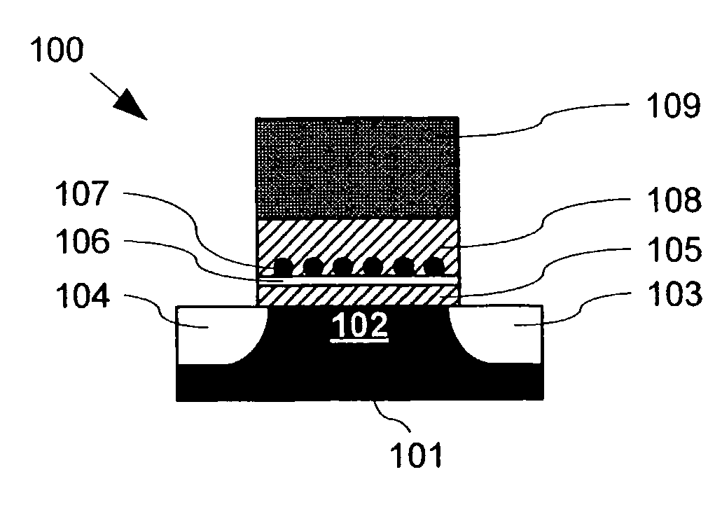
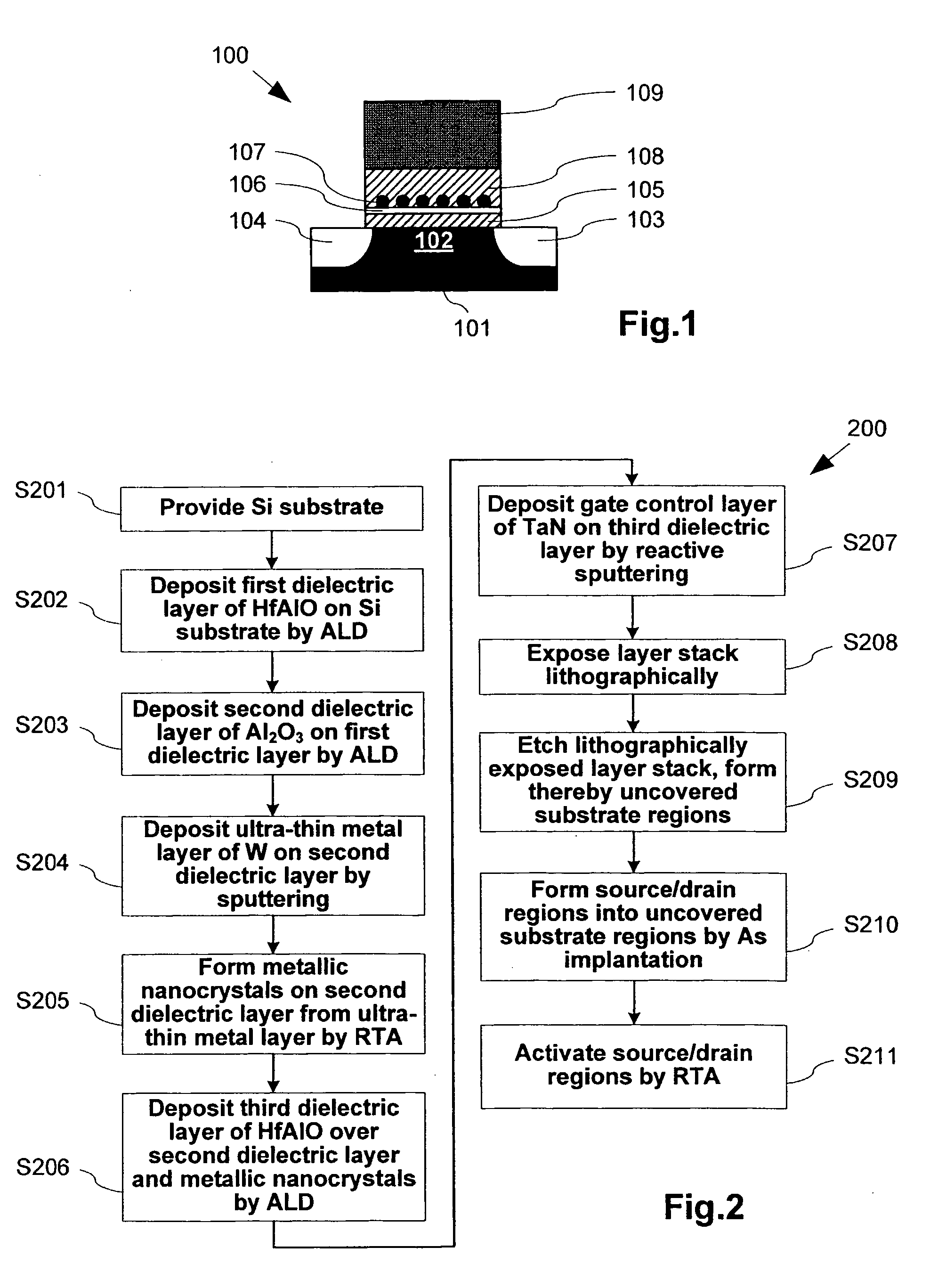
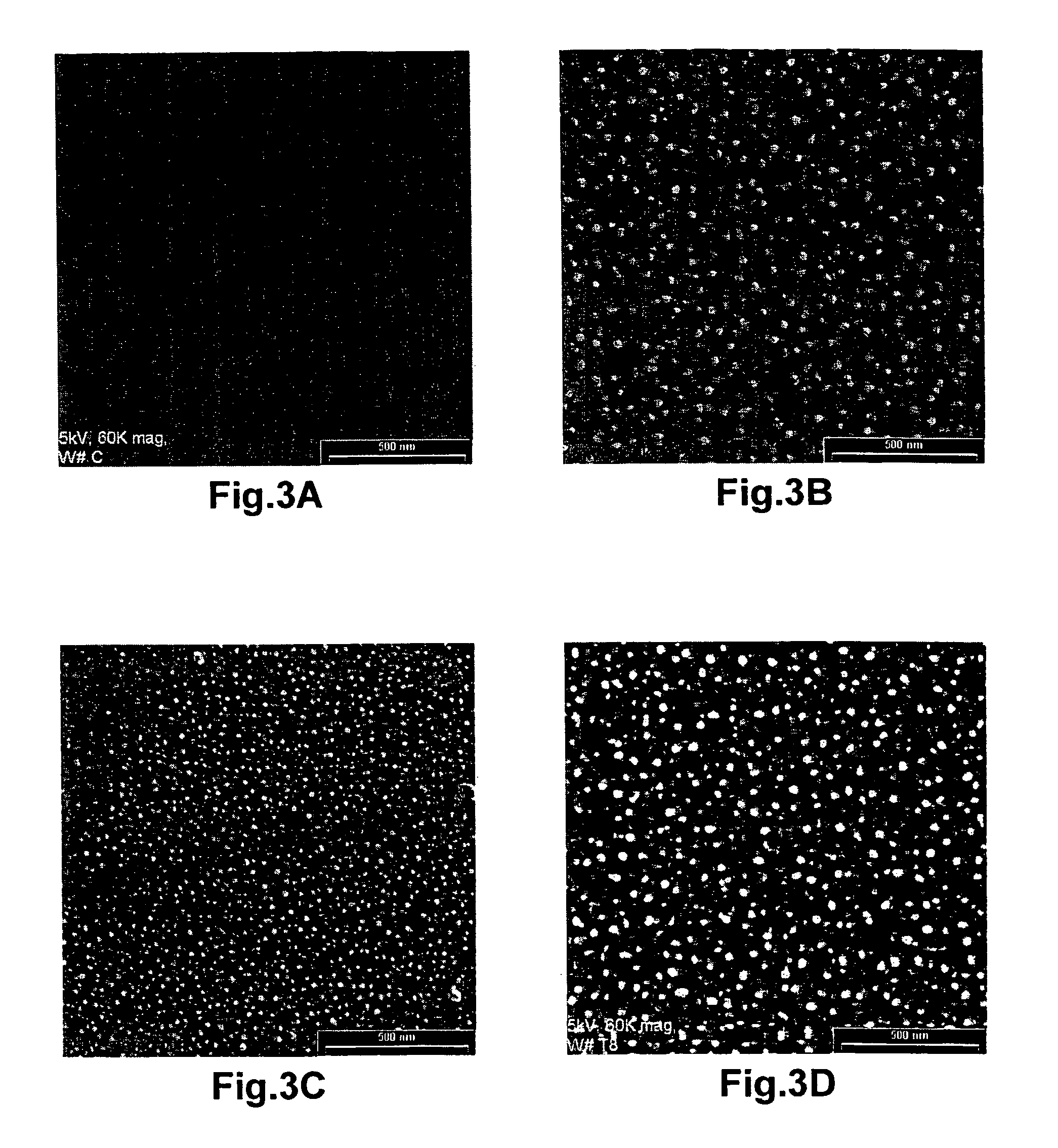
[0038]In the following detailed description of the invention, reference is made to the accompanying drawings which form a part hereof, and in which are shown, by way of illustration only, specific embodiments of this invention. In the drawings, like numerals describe substantially similar components throughout the several views.

[0039]The term substrate used in the following description refers to any doped and / or undoped semiconductor structure that has an exposed surface for the formation of an integrated circuit. Such a semiconductor structure may also comprise other layers that have been fabricated thereupon. Further, the terminals associated with the terms source and drain are determined by operating conditions of the nonvolatile flash memory device formed as a transistor, i.e. the terms source and drain are interchangeable. Additionally, the nonvolatile flash memory device described herein may be part of an arrayed memory, and may further comprise appropriate circuitry for drivi...


PUM


Abstract

A method of producing metallic nanocrystals (107) embedded in high-k dielectric material as well as a nonvolatile flash memory device (100) comprising a discrete charge carrier storage layer, the discrete charge carrier storage layer comprising metallic nanocrystals (107) embedded in high-k dielectric material. In the method described in this invention, firstly an ultra-thin metal film is deposited over a first (105) and a second (106) dielectric layer including high-k dielectric material provided on a substrate (101). Then, the ultra-thin metal film is annealed for forming the metallic nanocrystals (107) on the second dielectric layer (106). Finally, the second dielectric layer (106) and the metallic nanocrystals (107) are covered with a third dielectric layer (108) of high-k dielectric material for forming metallic nanocrystals (107) embedded in high-k dielectric material. The first (105), second (106) and third (108) dielectric layers together with the embedded metallic nanocrystals (107) as the discrete charge carrier storage layer form the nonvolatile flash memory device (100).

Description

FIELD OF THE INVENTION[0001]This invention relates generally to nonvolatile flash memory devices. In particular, this invention relates to a nonvolatile flash memory device comprising a discrete charge storage layer having metallic nanocrystals embedded in high-k dielectric material. The invention also relates to the fabrication of nonvolatile flash memory devices using metallic nanocrystals embedded in high-k dielectric material as a floating gate.BACKGROUND OF THE INVENTION[0002]In recent years, the demand for high density and high performance nonvolatile memory devices has increased to meet the requirements of a range of modern microprocessor-based devices which currently run a variety of functions within cars, personal and portable computers, voice recorders, mobile phones, digital cameras, other wireless products, and industrial control systems. For the future, the “International Technology Roadmap of Semiconductors” (ITRS) 2003 shows that the scale down of nonvolatile flash me...

Claims


Application Information

Patent Timeline
IPC IPC(8): H01L29/792H01L21/336
CPCB82Y10/00H01L21/28273H01L29/7887H01L29/513H01L29/42332H01L29/40114
Inventor SAMANTA, SANTANU KUMARYOO, WON JONG
Owner NAT UNIV OF SINGAPORE
Why Eureka
Try Eureka