Electrophoretic display device

a display device and display device technology, applied in the direction of instruments, static indicating devices, etc., can solve the problems of increasing the area per pixel, increasing the necessary space, complicated lines, etc., and achieve the effect of preventing the degradation of yield and high precision

Inactive Publication Date: 2009-07-30
E INK CORPORATION
View PDF2 Cites 17 Cited by
  • Summary
  • Abstract
  • Description
  • Claims
  • Application Information

AI Technical Summary

Benefits of technology

[0009]An advantage of some aspects of the invention is that it provides an electrophoretic display device capable of realizing high precision and preventing yield from deteriorating.
[0011]According to the invention, in the electrophoretic display device including the memory circuit and the switch circuit in each of the pixels, since the first power source line and the second power source line connected to the memory circuit cross each other at the first position and the first control line and the second control line connected to the switch circuit cross each other at the second position, it is possible to shorten the lines which are longitudinally crossed in each of the pixels. Accordingly, since a space occupied by the lines in each of the pixels can be reduced, it is possible to form a high-precision pixel. In addition, by reducing the space occupied by the lines in each of the pixels, since a margin is provided to the arrangement of the components in each of the pixels in the same resolution and a margin is provided to a distance between the lines, it is possible to prevent yield from deteriorating due to the short circuit or static electricity in the process of manufacturing the electrophoretic display device.
[0013]According to the invention, since each of the pixels has a rectangular shape in plan view, the first position corresponds to a first corner of the four corners of each of the pixels, and the second position corresponds to a second corner opposing the first corner of the four corners of each of the pixels, the connection position of the memory circuit and the connection position of the switch circuit can be divided into opposing corners of the pixels. Accordingly, it is possible to prevent the positions of the lines from being concentrated on predetermined points and thus disperse the lines in each of the pixels.
[0017]According to the invention, since at least one of the first power source line, the second power source line, the first signal line and the second signal line is shared by the adjacent pixels, it is possible to suppress the number of the first power source line, the second power source line, the first signal line and the second signal line and widen a space in each of the pixels. Accordingly, since a margin is provided to the arrangement of the lines in each of the pixels, it is possible to prevent yield from deteriorating due to the short circuit or static electricity in a manufacturing process.
[0019]According to the invention, since the arrangements of the pixels sharing the line in plan view are linearly symmetrical with respect to the line shared by the arrangements, it is possible to suppress the number of the first power source line, the second power source line, the first signal line and the second signal line without significantly changing the arrangement of the lines in each of the pixels.

Problems solved by technology

If the lines from the global lines are arranged to be longitudinally crossed, the connection between the components needs to avoid the lines, the lines become complicated, and a necessary space is increased.
In particular, since a wiring area is increased, an area per pixel is increased and high precision cannot be realized.
In this case, since particles may be attached between the lines and a short circuit may occur in a manufacturing process, yield may deteriorate.

Method used


Image

  • Electrophoretic display device
  • Electrophoretic display device
  • Electrophoretic display device

Examples


Embodiment Construction

[0030]Hereinafter, an embodiment of the invention will be described with reference to the accompanying drawings. In the present embodiment, for example, an electrophoretic display device driven by an active matrix method will be described. In each view used for following description, the scales or the numbers of the actual structures are differentiated from each other in order to recognize the configurations.

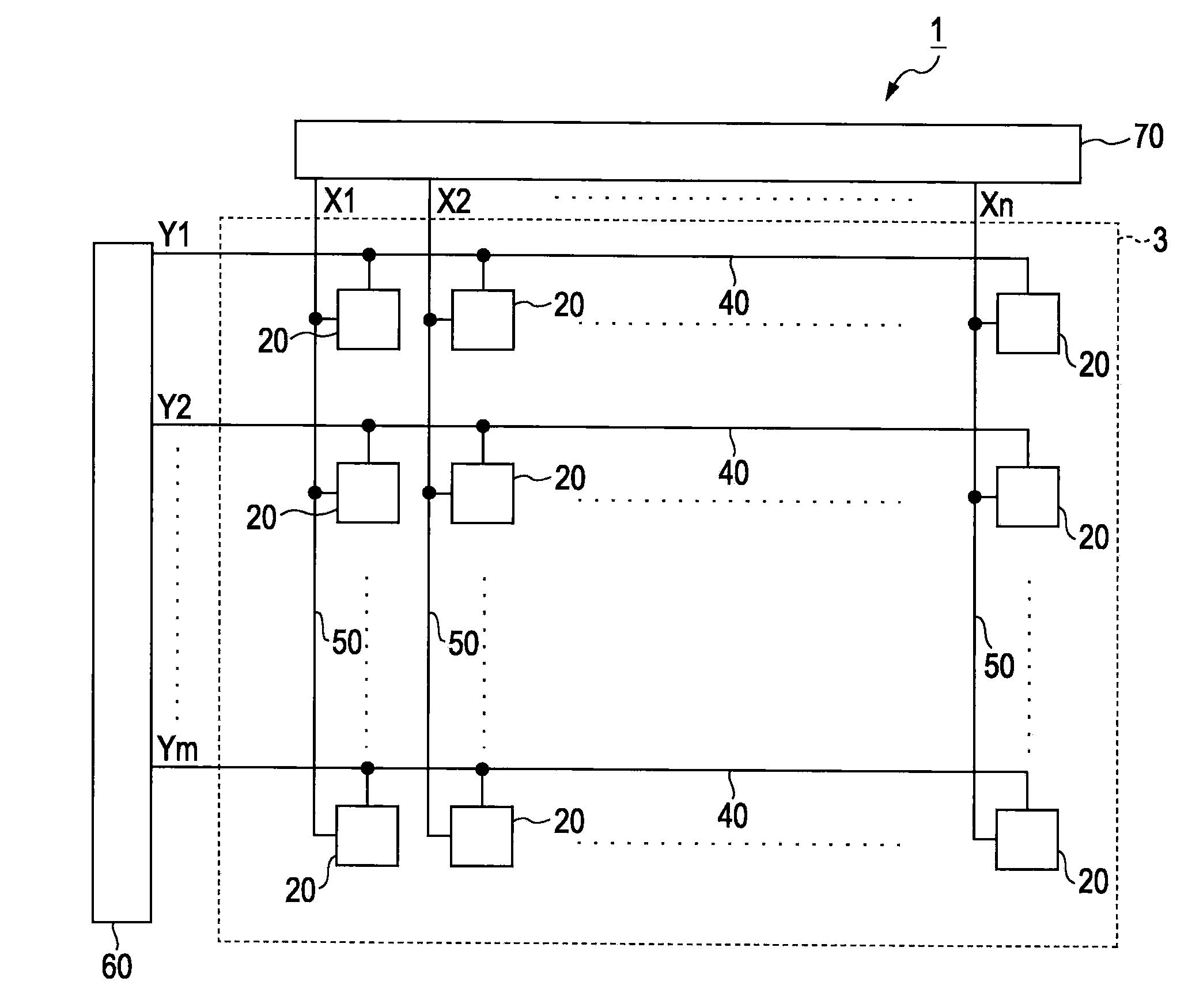
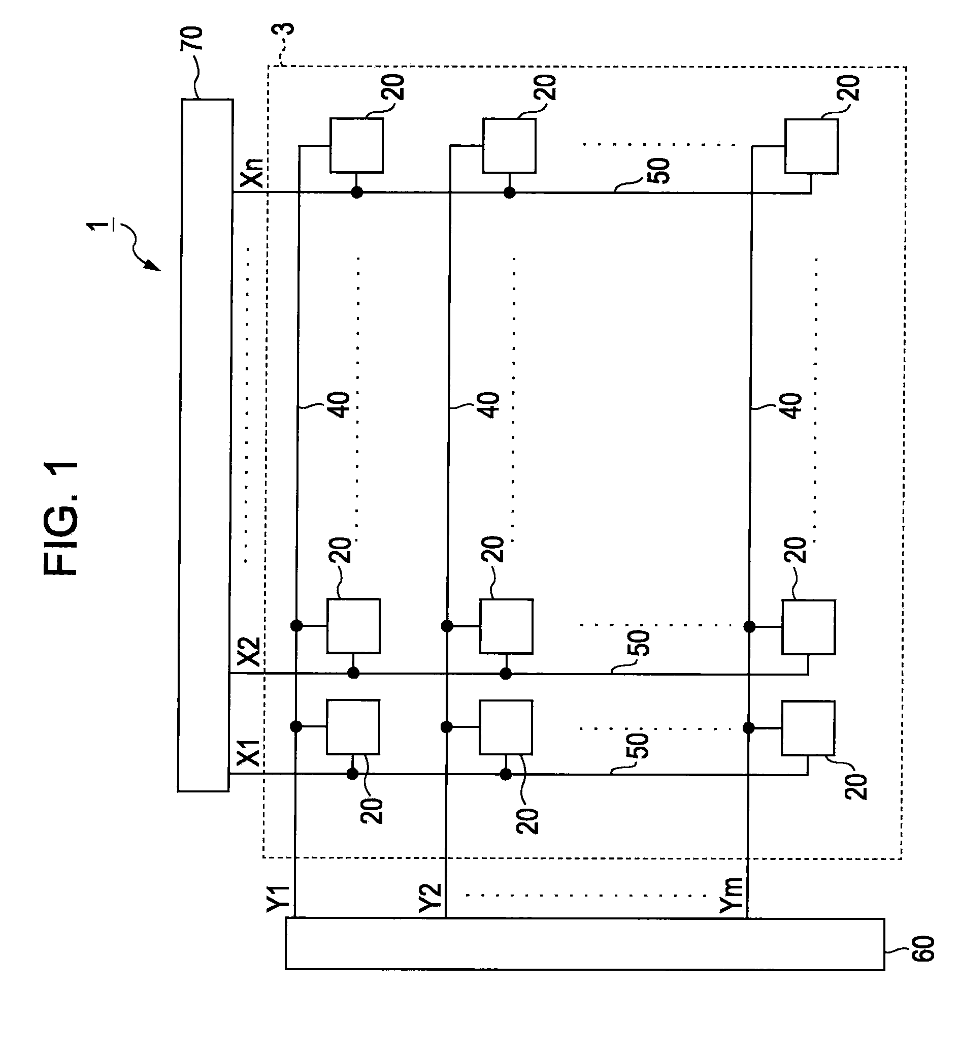
[0031]FIG. 1 is a schematic diagram of an electrophoretic display device 1 according to a first embodiment of the invention. The electrophoretic display device 1 includes a display unit 3 in which a plurality of pixels 20 are arranged, a scan line driving circuit 60 and a data line driving circuit 70.

[0032]In the display unit 3, a plurality of scan lines 40 (Y1, Y2, . . . , Ym) extending from the scan line driving circuit 60 and a plurality of data lines 50 (X1, X2, . . . , and Xn) extending from the data line driving circuit 70. Pixels 20 are arranged on intersections between t...


PUM


Abstract

An electrophoretic display device includes a pair of substrates, a pixel, a first electrode being formed on one of the substrates for the pixel, a second electrode being formed on the other of the substrates, and an electrophoretic element which is held between the first electrode and the second electrode. The pixel includes a pixel switching element which is connected to a scan line and a data line, a memory circuit which is connected to the pixel switching element, and a switch circuit which is interposed between the memory circuit and the first electrode. The memory circuit is connected with a first power source line and a second power source line, and the switch circuit is connected with a first control line and a second control line. The first power source line and the second power source line cross each other at a first position of the pixel, and the first control line and the second control line cross each other at a second position of the pixel.

Description

BACKGROUND[0001]1. Technical Field[0002]The present invention relates to an electrophoretic display device.[0003]2. Related Art[0004]An active matrix type electrophoretic display device includes switching transistors and memory circuits in pixels (for example, see JP-A-2005-114822). In the display device described in JP-A-2005-114822, an electrophoretic element including a plurality microcapsules, in which charged particles are included, are adhered on a device substrate on which pixel switching transistors or pixel electrodes are formed and the electrophoretic element is sandwiched between the device substrate and a counter substrate on which counter electrodes are mounted.[0005]Each of the pixel circuits of the electrophoretic display device is preferably laid out such that a circuit area is reduced in order to realize high-precision display. Accordingly, it is preferable that the number of lines in each of the pixel circuits is small. For example, in each of the pixel circuits of...

Claims


Application Information

Patent Timeline
Patent Type & Authority Applications(United States)
IPC IPC(8): G09G3/34
CPCG09G2300/0809G09G2300/0857G09G2330/02G09G3/344G09G2300/0426G09G2330/04
Inventor MURAYAMA, TETSUROSHIMODAIRA, YASUHIRO
Owner E INK CORPORATION
Why Eureka
Try Eureka