Wafer position teaching method and teaching tool

Inactive Publication Date: 2009-08-06
YASKAWA DENKI KK
View PDF25 Cites 7 Cited by
  • Summary
  • Abstract
  • Description
  • Claims
  • Application Information

AI Technical Summary

Benefits of technology

[0019]According to the invention, sensing two or more external teaching tools arranged in a horizontally offset manner enables detection of the inclination of the processing equipment with respect to the robot, which in turn makes it possible to estimate the position of the semiconductor wafer with a high degree of accuracy.
[0020]Furthermore, by sensing the external teaching tools mounted on the front external wall of the equipment to estimate the position of the teaching tool, replacing the pre

Problems solved by technology

In some cases, however, it is difficult, or even impossible, to visually recognize the wafer disposed in a processing equipment or the like from the outside thereof.
In a conventional method, however, if the installation accuracy of a processing equipment with respect

Method used


Image

  • Wafer position teaching method and teaching tool
  • Wafer position teaching method and teaching tool
  • Wafer position teaching method and teaching tool

Examples


example 1

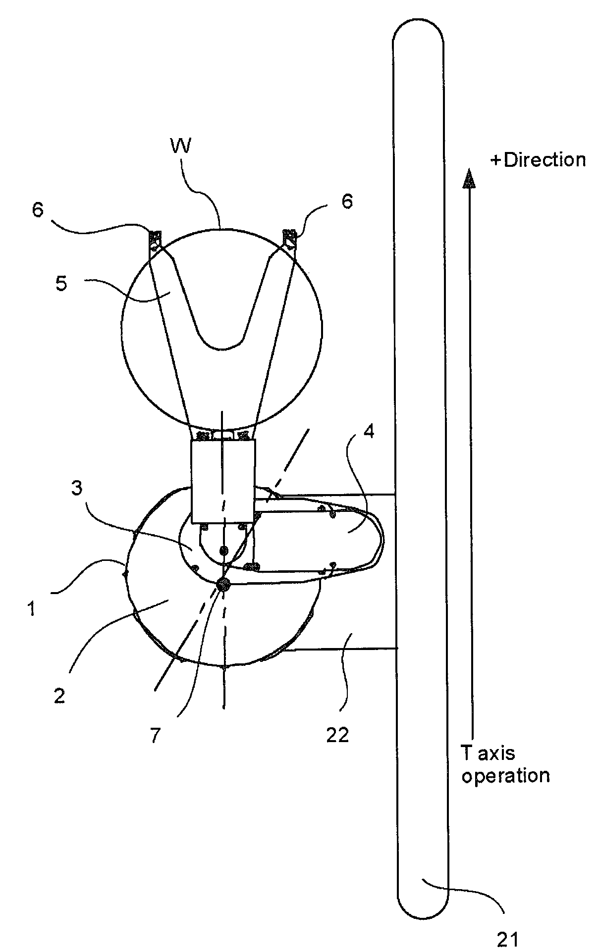
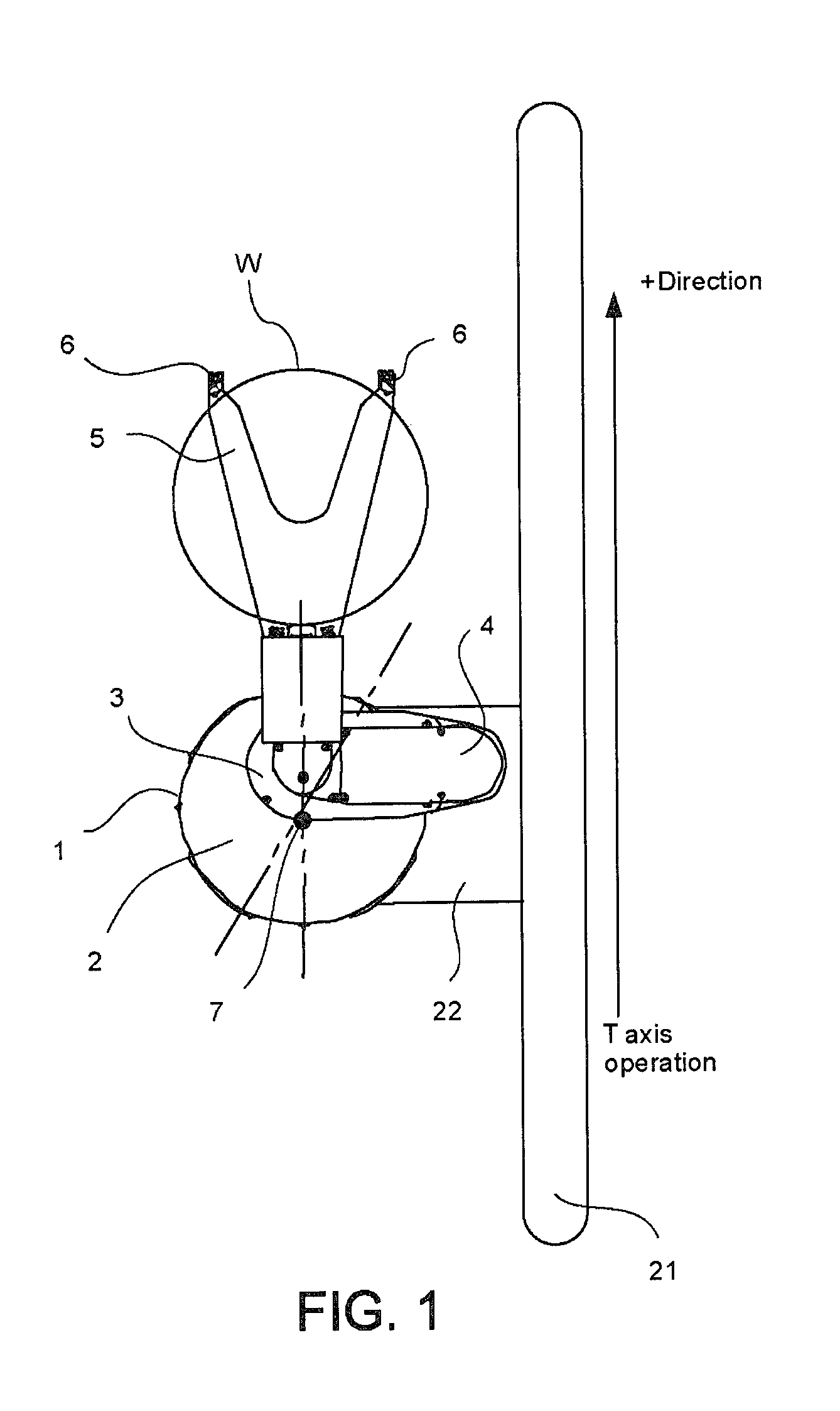
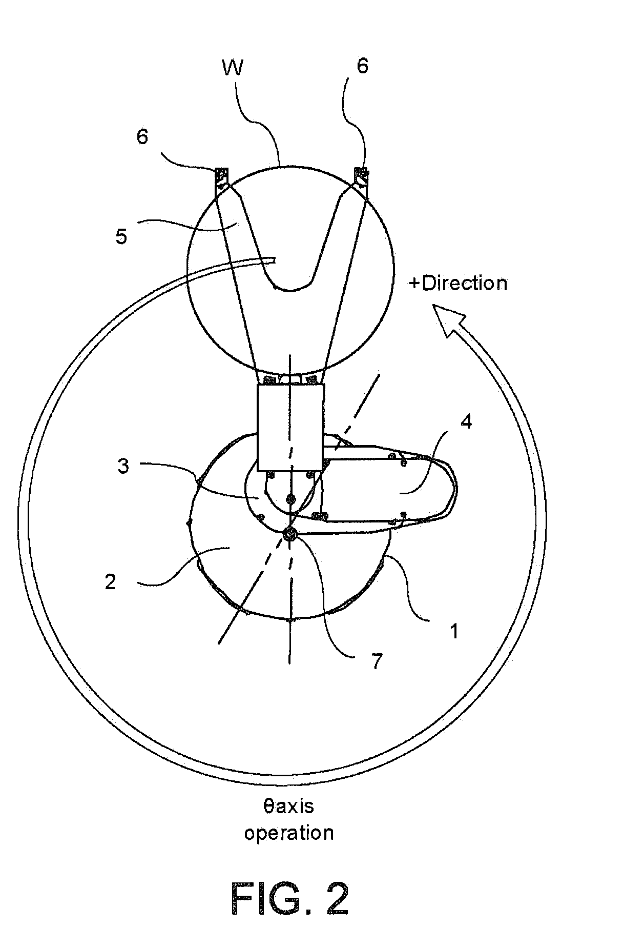
[0032]FIG. 1 is top view showing a robot of an embodiment according to the present invention. FIG. 4 is a side view thereof.

[0033]In FIG. 1, the reference numeral “1” denotes a horizontal articulated type robot for carrying a semiconductor wafer, and “W” denotes a semiconductor wafer to be carried by the robot. The robot 1 is equipped with a first arm 3 capable of rotating about a robot rotational center axis 7 of an elevating columnar support portion 2 in a horizontal plane, a second arm 4 attached to the tip end of the first arm 3 in a rotatable manner in a horizontal plane, and a wafer gripping portion 5 attached to the tip end of the second arm 4 in a rotatable manner in a horizontal plane. The wafer gripping portion 5 is formed into a Y-shaped hand for placing a semiconductor wafer W thereon and provided with a pair of transmission-type sensors 6 at the tip ends thereof. The reference numeral “21” denotes a traveling axis unit, and “22” denotes a traveling axis robot mount. The...


PUM


Abstract

In the wafer position teaching method for a wafer carrying system, a teaching tool is mounted at a position of the container or the processing equipment where the semiconductor wafer is to be set. The teaching tool is sensed by a sensor provided at a wafer gripping portion of the robot. Prior to sensing the teaching tool by the sensor, external teaching tools mounted on a front external wall of the processing equipment are sensed by the sensor to roughly estimate the position of the teaching tool. Based on the estimated position, the sensor approaches and senses the teaching tool to obtain the position of the semiconductor wafer. Thus, the wafer position can be taught precisely and automatically without causing interference, even when the frontage of processing equipment is narrow.

Description

RELATED APPLICATIONS[0001]This application is a continuation-in-part of an International Patent Application No. PCT / JP2006 / 313027, filed on Jun. 29, 2006. This application claims priority under 35 U.S.C. §119 to Japanese Patent Application No. 2005-206304 filed on Jul. 15, 2005. Each of the entire disclosures of these applications is incorporated herein by reference in its entirety.BACKGROUND OF THE INVENTION[0002]1. Field of the Invention[0003]The present invention relates to a method for teaching a position of a semiconductor wafer to a semiconductor wafer carrying robot, and more specifically to an external teaching tool for use in the method.[0004]2. Description of Related Art[0005]Conventionally, in the same manner as in a general industrial robot, a teaching operation of a semiconductor carrying robot has been performed by an operator by guiding the robot to a wafer to be carried while visually recognizing the wafer position. In some cases, however, it is difficult, or even im...

Claims


Application Information

Patent Timeline
IPC IPC(8): H01L21/68
CPCG05B2219/50125H01L21/681H01L21/67742G05B19/402G05B2219/37608G05B2219/40562H01L21/67259H01L21/67265H01L21/68707
Inventor ADACHI, MASARUKAWABE, MITSUNORI
Owner YASKAWA DENKI KK
Why Eureka
Try Eureka