Nonvolatile semiconductor memory device and method of manufacturing the same

Inactive Publication Date: 2009-08-13
RENESAS ELECTRONICS CORP
View PDF10 Cites 15 Cited by
  • Summary
  • Abstract
  • Description
  • Claims
  • Application Information

AI Technical Summary

Benefits of technology

[0016]According to the present invention, the erase gate is formed completely above the floating gate and does not face a side surface of the floating gate. In addition, both edge portions of the upper surface of the floating gate are closest to the erase gate, and an interval between a center portion of the upper surface and the erase gate is relatively large. Therefore, unnecessary coupling capacitance between the erase gate and the floating gate is eliminated. Since the coupling capacitance between the erase gate and the floating gate is reduced, the speeding-up of the data erasing operation is achieved and thus an erase efficiency is improved. In other words, the erase speed as well as the read speed can be improved.

Problems solved by technology

Therefore, the gate insulating film immediately under the control gate to which the high potential is applied cannot be made thin, from a viewpoint of reliability.

Method used


Image

  • Nonvolatile semiconductor memory device and method of manufacturing the same
  • Nonvolatile semiconductor memory device and method of manufacturing the same
  • Nonvolatile semiconductor memory device and method of manufacturing the same

Examples


modification example

5. Modification Example

[0108]A method of manufacturing the memory cell having the features shown in FIG. 4 is not limited to that described referring to FIGS. 11 to 49. Other manufacturing methods are possible.

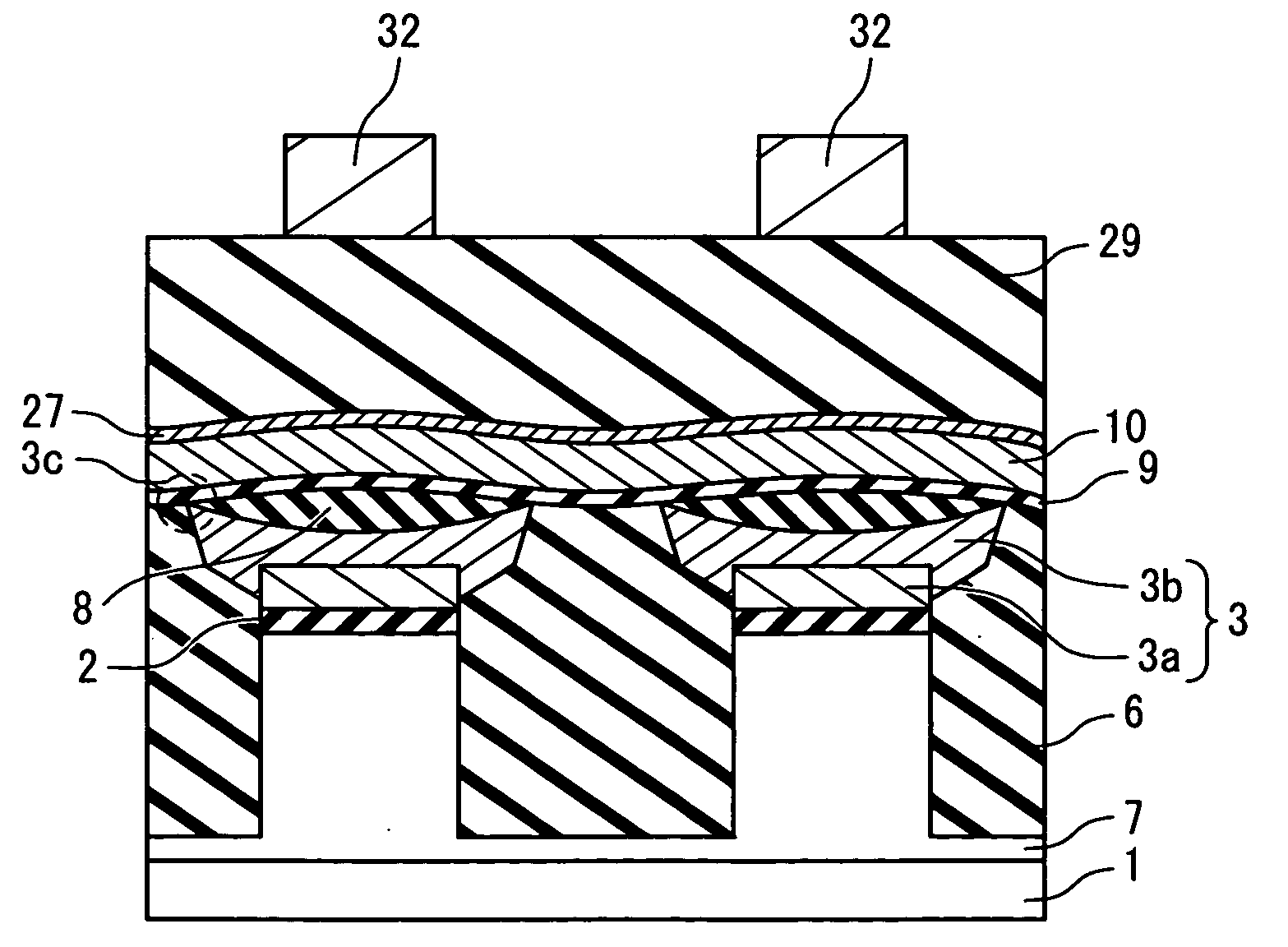
[0109]For example, FIG. 50 shows a structure disclosed in FIG. 4 of Japanese Laid-Open Patent Application JP-2001-230330. A device isolation oxide film 41 is formed on a silicon substrate 40 by the LOCOS method. A floating gate 43 is formed on the silicon substrate 40 through a gate oxide film 42. A selective oxide film 44 is formed on an upper surface of the floating gate 43 by a selective oxidation method. The selective oxide film 44 is made thick on the center portion of the floating gate 43 and thus the upper surface of the floating gate 43 is curved and has a dent. In FIG. 50, a side surface of the floating gate 43 overlaps the device isolation oxide film 41 and is exposed to an opening region on the device isolation oxide film 41.

[0110]Next, as shown in FIG. 51, an oxide...


PUM


Abstract

A nonvolatile semiconductor memory device has: a semiconductor substrate; a control gate and a floating gate that are formed side by side on a gate insulating film on a channel region in the semiconductor substrate; and an erase gate facing an upper surface of the floating gate and totally located above the upper surface of the floating gate. The upper surface of the floating gate includes a first side and a second side that face each other. A bottom surface of the erase gate is closer to the first side and the second side than the upper surface between the first side and the second side.

Description

INCORPORATION BY REFERENCE[0001]This application is based upon and claims the benefit of priority from Japanese patent application No. 2008-028578, filed on Feb. 8, 2008, the disclosure of which is incorporated herein in its entirely by reference.BACKGROUND OF THE INVENTION[0002]1. Field of the Invention[0003]The present invention relates to a split gate-type nonvolatile semiconductor memory device and a method of manufacturing the same. In particular, the present invention relates to a split gate-type nonvolatile semiconductor memory device provided with an erase gate and a method of manufacturing the same.[0004]2. Description of Related Art[0005]Flash memories and EEPROMs are known as electrically erasable / programmable nonvolatile semiconductor memory devices. A memory cell of such a nonvolatile semiconductor memory device is typically a transistor provided with a floating gate and a control gate. The control gate may be stacked on the floating gate or may be formed on at least a ...

Claims


Application Information

Patent Timeline
IPC IPC(8): H01L29/792H01L29/788
CPCG11C16/0433H01L21/28273H01L29/7881H01L27/11521H01L29/42328H01L27/115H01L29/40114H10B69/00H10B41/30
Inventor NAGAI, TAKAAKI
Owner RENESAS ELECTRONICS CORP
Why Eureka
Try Eureka