Image sensor with high conversion efficiency
a conversion efficiency and image sensor technology, applied in the field of image sensors, can solve the problems of reducing conversion efficiency, sensitivity reduction, crosstalk between pixels, etc., and achieve the effects of reducing crosstalk, reducing the amount of unneeded charge carriers, and reducing the absorption rate of such ligh
- Summary
- Abstract
- Description
- Claims
- Application Information
AI Technical Summary
Benefits of technology
Problems solved by technology
Method used
Image

Examples
Embodiment Construction
[0030]Embodiments of the present invention are described herein for a CMOS (complementary metal oxide semiconductor) image sensor (CIS) with a photodiode used as a photoelectric converter. However, the present invention is not restricted thereto, and the present invention may be practiced with other types of image sensors and with other types of photoelectric converters.
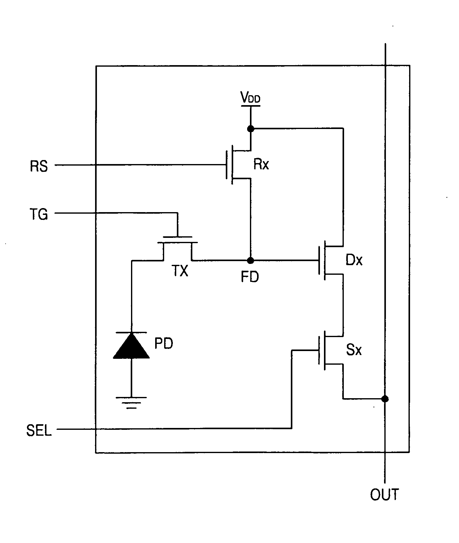
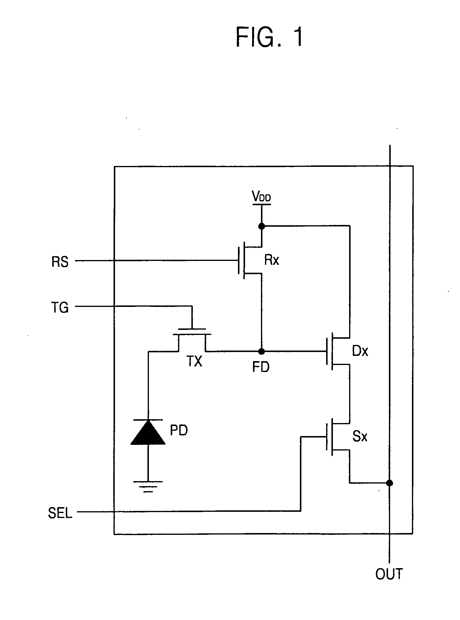
[0031]FIG. 1 shows an outline of an example unit pixel of an image sensor that is a CMOS image sensor for example. The example unit pixel of FIG. 1 includes a photoelectric converter which may be a photodiode PD for generating electric charge from received light. The unit pixel also includes a transfer transistor Tx that transfers such electric charge generated from the photodiode PD to a floating diffusion region FD in response to a transfer control signal TG.
[0032]In addition, the unit pixel includes a reset transistor Rx that periodically resets the floating diffusion region FD using a high power voltage VDD in re...
PUM
 Abstract
Description
Claims
Application Information