Electronic housing with a conductive plate, and method for manufacturing the same

a technology of conductive plates and electronic housings, which is applied in the direction of printed circuit board receptacles, electrical apparatus casings/cabinets/drawers, support structures, etc., can solve the problems of relatively narrow arrangement and unit thickness, and achieve the effect of simple production method

Active Publication Date: 2009-08-13
WEIDMULLER INTERFACE GMBH & CO KG
View PDF9 Cites 10 Cited by
  • Summary
  • Abstract
  • Description
  • Claims
  • Application Information

AI Technical Summary

Benefits of technology

[0013]It is also advantageous when the conductor connection housings at any rate, section by section, themselves constitute a part of the electronics housing because that contributes to an even narrower design.
[0014]The invention furthermore creates a particularly simple method for the production of an electronics housing that is characterized by the following steps: arrangement of a plurality of connector housings that receive conductor connections laterally with respect to the outer rim of the printed circuit board, and resiliently connecting or permanently soldering the conductor connections via contact areas such as fixed contacts upon the printed circuit board and fashioning a part of at least one sidewall of the electronics housing by arranging the printed circuit board with the conductor connection housings in the electronics housing.
[0015]In this way, one can in a simple manner, directly during the actual soldering procedure, arrange a part of the electronics housing itself together on the printed circuit board so that the conductor connections will lie in a well-protected position during the actual further assembly of the electronics housing.

Problems solved by technology

Unfortunately, this prevents the arrangement from being relatively narrow, because the height of the printed circuit board and the height of the connections for the conductors unduly increase the thickness of the unit.

Method used


Image

  • Electronic housing with a conductive plate, and method for manufacturing the same
  • Electronic housing with a conductive plate, and method for manufacturing the same
  • Electronic housing with a conductive plate, and method for manufacturing the same

Examples


Embodiment Construction

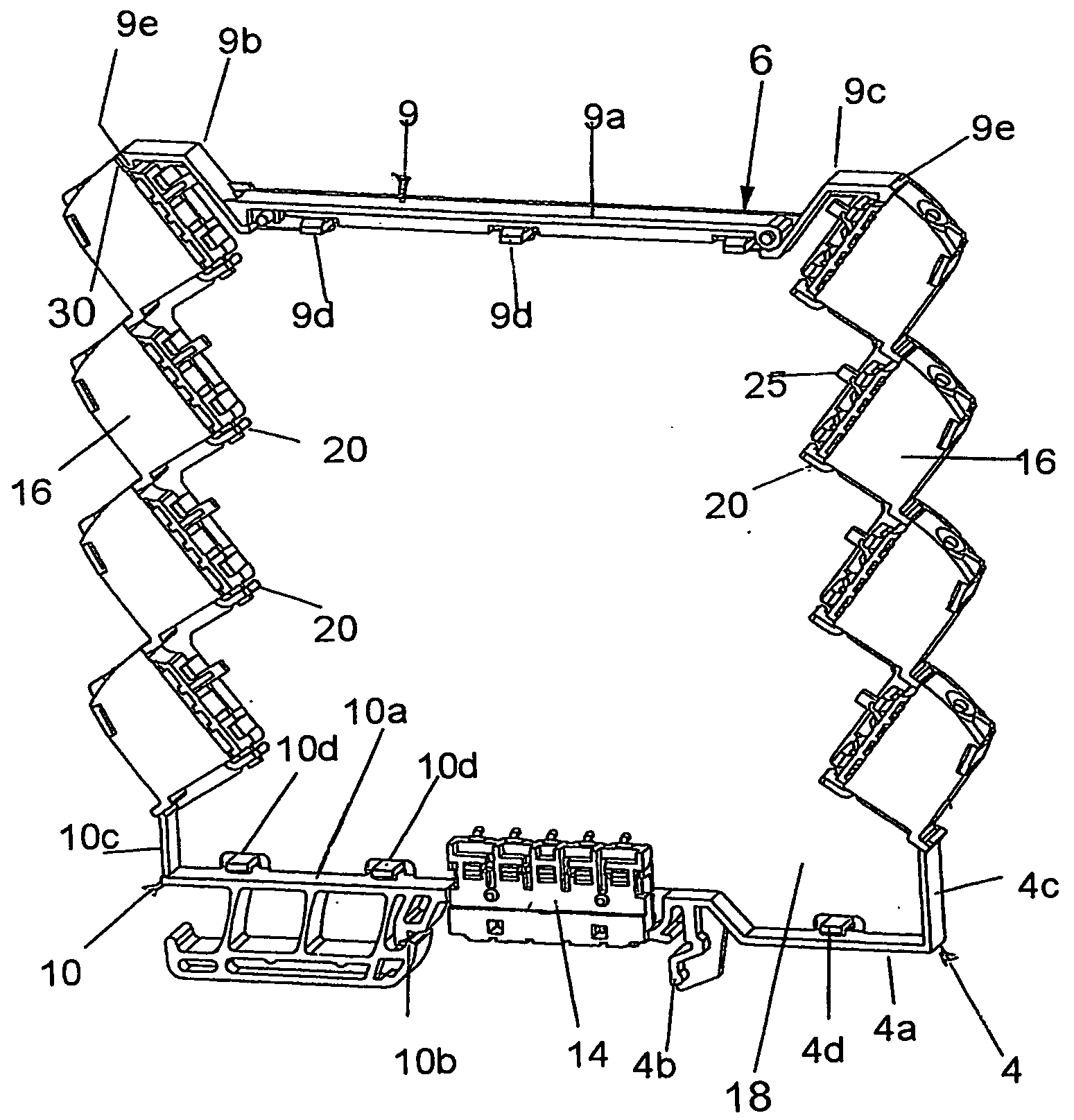
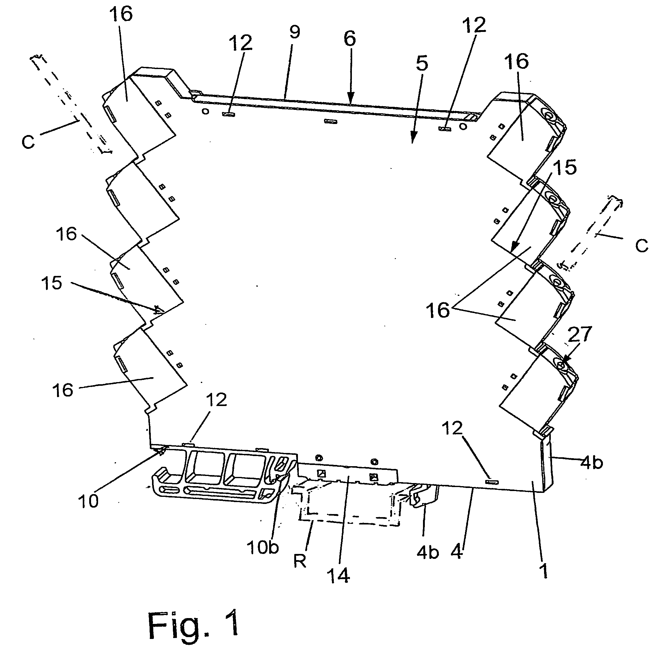
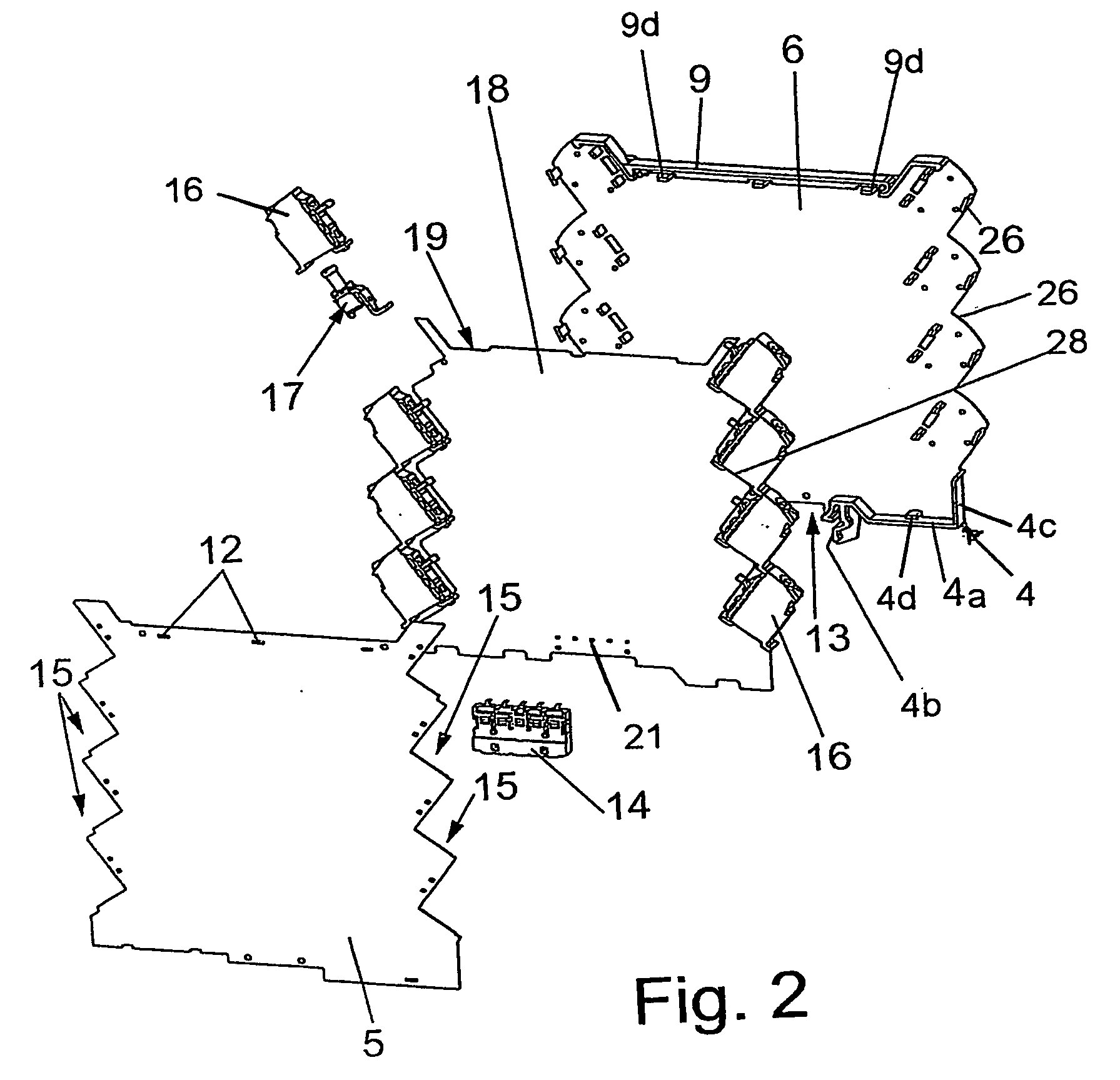
[0023]Referring first more particularly to FIGS. 1 and 2, the printed circuit arrangement 1 has a generally rectangular configuration including a front wall 5, a rear wall 6, a top wall 9, and bottom wall members 4 and 10 separated by the space 13. The printed circuit board 18 is arranged contiguously between and parallel with the front wall 5 and the rear wall 6. Supported on the printed circuit board 18 are a plurality of rectangular relatively-thin connector housings 16 provided with moveable connectors 17 that serve to connect external conductors C with circuits printed on the printed circuit board 18 via fixed contacts 20. The bottom members 4 and 10 are provided with foot portions 4a and 10a that serve to connect the assembly to a mounting rail R having a generally inverted hat-shaped configuration. Mounted on the bottom edge of the assembly in the opening 13 is a bus connector 14 that is adapted for connection with electrical circuits associated with the stationary mounting r...


PUM

PropertyMeasurementUnit
thicknessesaaaaaaaaaa
thicknessaaaaaaaaaa
electrically-insulatingaaaaaaaaaa

Abstract

A printed circuit board arrangement and method includes a planar generally-rectangular vertically-arranged printed circuit board having front and rear surfaces terminating in a peripheral edge, at least one of the front and rear surfaces having a conductive printed circuit thereon. The printed circuit board has a vertical side edge portion containing a recess, and arranged adjacent the recess is a fixed contact connected with a conductor portion of the printed circuit. A relatively narrow conductor housing arranged outside the peripheral edge of the printed circuit board is mounted in the recess with a movable contact carried by the housing in electrical engagement with the fixed contact. The connector housing is supported by a rear wall mounted on the rear surface of the printed circuit board, and by a resilient clip on the connector housing that engages the printed circuit board adjacent the recess.

Description

REFERENCE TO RELATED APPLICATIONS[0001]This application is related to the Heggemann et al applications Ser. No. ______ filed ______ entitled “Connector Apparatus With Code Means, and Method of Assembling the Same” [Docket 19929], Ser. No. ______ filed ______ entitled “Housing for Electrical Components” [Docket 19934], and Ser. No. ______ filed entitled “Stackable Electronic Housing With Male or Female Connector Strips” [Docket No. 19937].BACKGROUND OF THE INVENTION[0002]1. Field of the Invention[0003]A printed circuit board arrangement and method includes a planar generally-rectangular vertically-arranged printed circuit board having front and rear surfaces terminating in a peripheral edge, at least one of the front and rear surfaces having a conductive printed circuit thereon. The printed circuit board has a vertical side edge portion containing at least one recess, and arranged adjacent said recess is a fixed contact connected with a conductor portion of the printed circuit. A rel...

Claims


Application Information

Patent Timeline
Patent Type & Authority Applications(United States)
IPC IPC(8): H01R12/00H01R9/00
CPCH01R9/2625H05K1/182H05K3/0052H05K3/3405Y10T29/49149H05K2201/09145H05K2201/10189H05K2201/10446H05K7/1428
Inventor HEGGEMANN, CHRISTIANOESTERHAUS, JENSBOENSCH, MATTHIASNIGGEMANN, MATTHIASLENSCHEN, MICHAELFEHLING, STEPHANDIEKMANN, TORSTEN
Owner WEIDMULLER INTERFACE GMBH & CO KG
Why Eureka
Try Eureka