Organic el display module and manufacturing method of the same

a technology of organic el and display modules, which is applied in the direction of instruments, computing, electric digital data processing, etc., can solve the problems of inability to measure pixel currents for all effective pixels, inability to meet the requirements of measurement time, so as to prevent the occurrence of display unevenness and reduce the measurement time of data used in the correction of display unevenness

Active Publication Date: 2009-08-20
GLOBAL OLED TECH
View PDF8 Cites 48 Cited by
  • Summary
  • Abstract
  • Description
  • Claims
  • Application Information

AI Technical Summary

Benefits of technology

[0023]According to the present invention, a measurement time of data used in correcting display unevenness can be reduced, and, further, influence of a resistance component in a power supply line extending in the vertical direction can be removed, to thereby prevent occurrence of display unevenness.

Problems solved by technology

Variance in the Vth or the μ of the drive TFT 1 of the pixels 14 in the display panel (pixel matrix: effective pixel region) usually results in uneven brightness of the display panel.
However, in this case, resistance in the vertical power supply line which connects between power supply lines of the horizontal lines and supplies power to these horizontal power supply lines must be negligible.
However, the current to be measured changes due to, for example, wiring resistance and stray capacitance, and gradually increases after the pixel data are written in the storage capacitor C. As such, the current must be measured after the current is sufficiently stabilized, and a considerable amount of time is required to measure pixel currents for all effective pixels after stabilization.
As shown in this figure, a considerable amount of time is required for stabilization of the current flowing in a PVdd in each of the pixels.
In addition, an unevenness correction value does not usually take into consideration a supply voltage drop at a pixel circuit.
The accuracy of such correction therefore becomes worse as the voltage to be supplied to the pixel is reduced.
However, when a vertical PVDD line includes a resistance component, uneven distribution of supply voltages occurs in the vertical direction, and this causes display unevenness.

Method used


Image

  • Organic el display module and manufacturing method of the same
  • Organic el display module and manufacturing method of the same
  • Organic el display module and manufacturing method of the same

Examples


specific examples

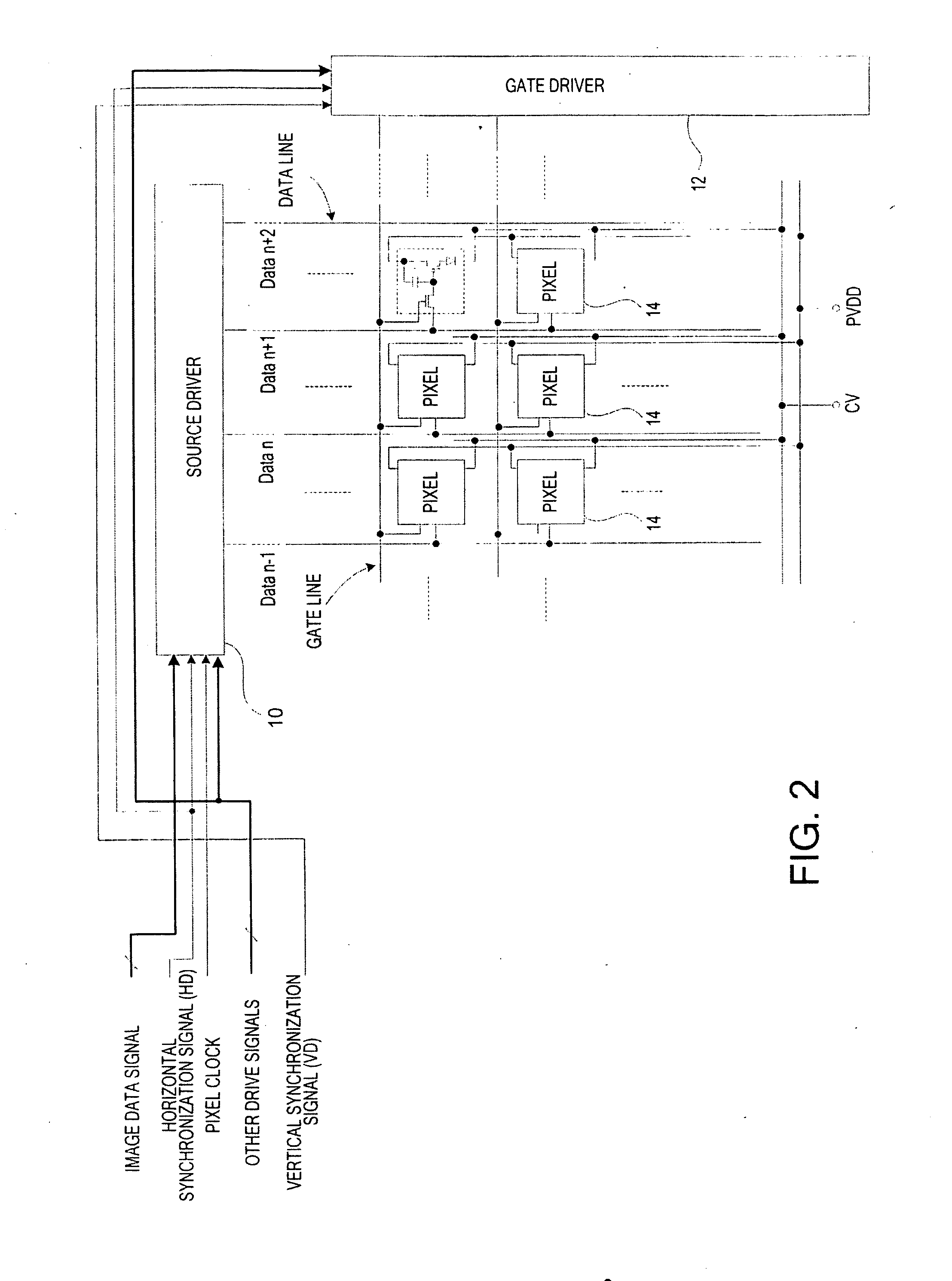
[0059]FIG. 10A and FIG. 10B show example module configurations during measurement and at the time of shipment, respectively, in which PVDD terminals 35 are provided only on the left side and the PVDD power supply is connected to those PVDD terminals. In the example shown in FIG 10B, at the time of shipment, the PVDD terminals 35 are connected to a power supply terminal 34 of a TCON and image-processing board (printed circuit board (PCB)) 30 using a coupling flexible cable (FPC) 32. An AFC (anisotropically-conductive film) is preferably used to connect the FPC 32 to an array substrate (panel) 38 that constitutes a display panel, and a connector or soldering is preferably used to connect the FPC 32 to the TCON and image process board 30 in order to reduce connection resistance. When vertical PVDD lines are provided on both sides of the panel, at the time of shipment, all the right side horizontal PVDD lines 35 are coupled using FPC or the like and are at the same time connected to the...


PUM


Abstract

On a panel, a plurality of PVDD lines, each of which corresponds to a horizontal line of pixels and supplies power to the pixels of the horizontal line, are provided. A voltage drop correction unit that obtains a voltage drop before reaching the pixel, based on resistance in the plurality of power supply lines and currents flowing therein, and corrects display data so as to cancel the obtained voltage drop of the pixel. A display unevenness correction unit that corrects uneven brightness caused by a variation in a TFT characteristic of the pixel by performing a calculation using display data of the pixel and obtained correction data of the pixel.

Description

CROSS-REFERENCE TO RELATED APPLICATION[0001]This application claims priority of Japanese Patent Application No. 2008-038857 filed Feb. 20, 2008 which is incorporated herein by reference in its entirety.FIELD OF THE INVENTION[0002]The present invention relates to an active organic EL display module in which pixels are arranged in a matrix, each pixel having an organic EL element for display use and a TFT that controls current supply to the organic EL element.BACKGROUND OF THE INVENTION[0003]FIG. 1 shows a configuration of a circuit of a single pixel (pixel circuit) in a basic active organic EL display device. FIG. 2 shows one example of a configuration of a display module and an input signal.[0004]As shown in FIG. 1, a pixel circuit is composed of a selection TFT 2 in which either a source or a drain is connected to a data line Data and a gate is connected to a gate line Gate, a drive TFT 1 having a gate connected to either the source or the drain of the selection TFT 2 and a source ...

Claims


Application Information

Patent Timeline
IPC IPC(8): G09G3/30
CPCG09G3/3233G09G2310/0218G09G2330/028G09G2320/0285G09G2330/021G09G2320/0223
Inventor MIZUKOSHI, SEIICHIMORI, NOBUYUKIKOHNO, MAKOTOONOMURA, KOUICHI
Owner GLOBAL OLED TECH
Why Eureka
Try Eureka