Ceramic electronic component, manufacturing method of ceramic electronic component, and packaging method of ceramic electronic components

a technology of electronic components and manufacturing methods, applied in the manufacture of final products, lighting and heating apparatus, lighting support devices, etc., can solve the problems of variation in electrical characteristics, inability to visually recognize directions, and inability to so as to improve the accuracy of determination of color differences and accurately determine the direction of conductors

Active Publication Date: 2009-08-20
TDK CORPARATION
View PDF5 Cites 37 Cited by
  • Summary
  • Abstract
  • Description
  • Claims
  • Application Information

AI Technical Summary

Benefits of technology

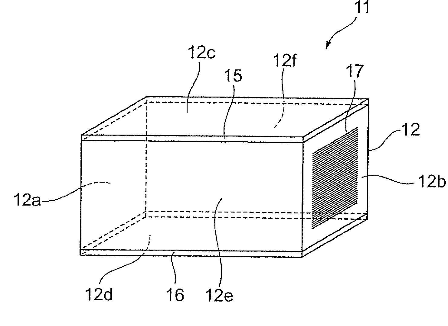
[0025]In the present invention, when the side face with the discrimination layer of the chip element body is set as a side face to become parallel to the conductor arrangement direction or as a side face to become perpendicular to the conductor arrangement direction, it becomes easy to determine the conductor arrangement direction in the chip element body, based on the discrimination layer. As a result, the ceramic electronic components can be packaged with their conductor arrangement directions being aligned.
[0026]Preferably, the determination step comprises discriminating the difference between the colors of the at least one side face out of the third and fourth side faces, and the discrimination layer, based on a difference between luminance values of the at least one side face out of the third and fourth side faces, and the discrimination layer. In this case, the accuracy is improved for determination of the difference of colors and it is thus feasible to accurately determine the conductor arrangement direction.

Problems solved by technology

Therefore, the electrical characteristics of the ceramic electronic component differ depending upon the opposing direction of the conductor layers relative to the mounting substrate, which causes a problem of variation in the electrical characteristics.
This is not limited only to the configuration wherein the plurality of conductor layers are opposed to each other inside the chip element body, but also applies to any ceramic electronic component in which a conductor is formed inside a chip element body, with the problem that its electrical characteristics vary depending upon an arrangement direction of the conductor.
In the completed ceramic electronic component, however, the conductor inside the chip element body is usually covered by a ceramic and external electrodes and thus the direction thereof cannot be visually recognized.

Method used


Image

  • Ceramic electronic component, manufacturing method of ceramic electronic component, and packaging method of ceramic electronic components
  • Ceramic electronic component, manufacturing method of ceramic electronic component, and packaging method of ceramic electronic components
  • Ceramic electronic component, manufacturing method of ceramic electronic component, and packaging method of ceramic electronic components

Examples


examples

[0086]The present invention will be described below in more detail with examples thereof, but it should be noted that the present invention is by no means intended to be limited to these examples.

[0087]Examples 1-12 represent the ceramic electronic components manufactured by the manufacturing method of ceramic electronic components according to the aforementioned embodiment and Comparative Example 1 represents a ceramic electronic component without the discrimination layers manufactured without the discrimination layer forming step in the manufacturing method of ceramic electronic components according to the foregoing embodiment.

[0088]FIG. 7 shows the materials of the ceramic green layers and the measurement results with a spectrophotometer in Comparative Example 1 and Examples 1-12. The measurement results with the spectrophotometer are expressed by the CIE 1976 L*a*b* (CIELAB). The spectrophotometer used was micro spectrophotometer VSS 400 available from Nippon Denshoku Industries...


PUM

PropertyMeasurementUnit
distanceaaaaaaaaaa
distanceaaaaaaaaaa
coloraaaaaaaaaa

Abstract

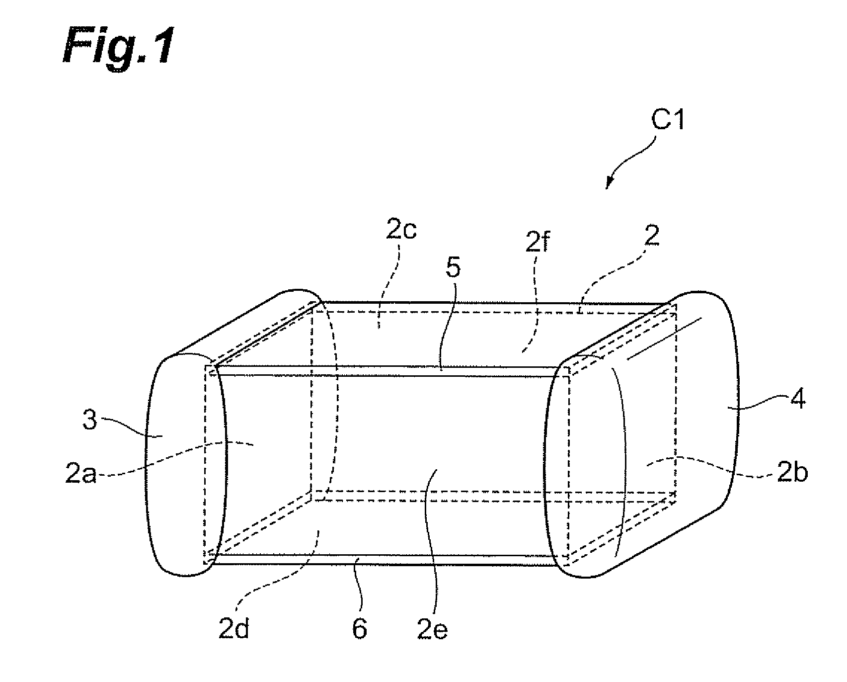
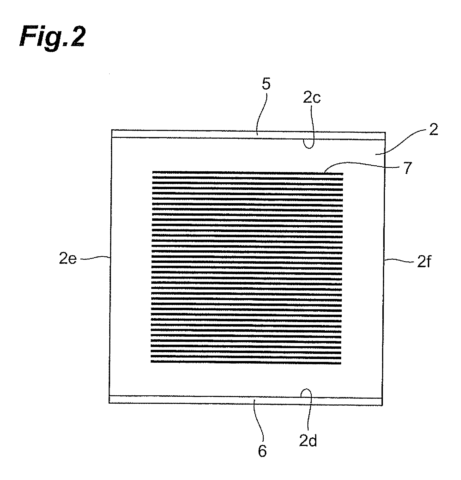
A ceramic electronic component has a chip element body having a conductor arranged inside, external electrodes, and a discrimination layer. The chip element body has first and second end faces facing each other, first and second side faces being perpendicular to the first and second end faces and facing each other, and third and fourth side faces being perpendicular to the first and second end faces and to the first and second side faces and facing each other. The external electrodes are formed on the first and second end faces, respectively, of the chip element body. The discrimination layer is provided on at least one side face out of the first side face and the second side face in the chip element body. The chip element body is comprised of a first ceramic. The discrimination layer is comprised of a second ceramic different from the first ceramic and has a color different from that of the third and fourth side faces.

Description

BACKGROUND OF THE INVENTION[0001]1. Field of the Invention[0002]The present invention relates to a ceramic electronic component, and a manufacturing method and packaging method thereof.[0003]2. Related Background Art[0004]There is a known ceramic electronic component having a chip element body formed in a rectangular parallelepiped shape, a plurality of conductor layers arranged so as to be opposed to each other inside the chip element body, and external electrodes formed on respective end faces of the chip element body. The ceramic electronic components of this configuration, after manufactured, are housed in respective recesses formed in a packaging material (cf. Japanese Patent Application Laid-open No. 61-217317).SUMMARY OF THE INVENTION[0005]For mounting each of the ceramic electronic components thus packaged, a suction carrier is used to suck an upper side face of the ceramic electronic component exposed from the recess of the packaging material, take the ceramic electronic co...

Claims


Application Information

Patent Timeline
Patent Type & Authority Applications(United States)
IPC IPC(8): H01G4/12B65B15/04H01G2/24H01G4/224
CPCH01G2/24H01G4/002H01G4/30H05K1/0269Y10T29/435H05K2201/10636H05K2203/161H05K2203/168H05K3/303Y02P70/50F21V21/30F21V19/02F21S8/003F21V17/12
Inventor IGUCHI, TOSHIHIROYOSHII, AKITOSHIGOSHIMA, AKIRAHASEBE, KAZUYUKI
Owner TDK CORPARATION
Why Eureka
Try Eureka