Manufacturing method of semiconductor device

a manufacturing method and semiconductor technology, applied in semiconductor devices, semiconductor/solid-state device details, electrical devices, etc., can solve the problems of reducing the fabrication yield of semiconductor devices of resin sealed semiconductor packages, cracking or the like in semiconductor chips, etc., to achieve enhanced heat radiation characteristic of semiconductor devices, the effect of enhancing the fabrication yield of semiconductor devices

Inactive Publication Date: 2009-08-27
RENESAS ELECTRONICS CORP
View PDF8 Cites 64 Cited by
  • Summary
  • Abstract
  • Description
  • Claims
  • Application Information

AI Technical Summary

Benefits of technology

[0026]According to the above representative embodiments, the fabrication yield of a semiconductor device can be enhanced.
[0027]In addition, the heat radiation characteristic of a semiconductor device can be enhanced.

Problems solved by technology

However, when the mold is so clamped that the upper terminals of a semiconductor chip are brought into contact with the upper die and the lower terminals of the semiconductor chip are brought into contact with the lower die, a problem arises.
When pressure is applied to the semiconductor chip from above and below, there is a possibility that cracking or the like occurs in the semiconductor chip.
This degrades the fabrication yield of semiconductor devices of a resin sealed semiconductor package type.

Method used


Image

  • Manufacturing method of semiconductor device
  • Manufacturing method of semiconductor device
  • Manufacturing method of semiconductor device

Examples


first embodiment

[0122]Description will be given to a semiconductor device in this embodiment with reference to drawings.

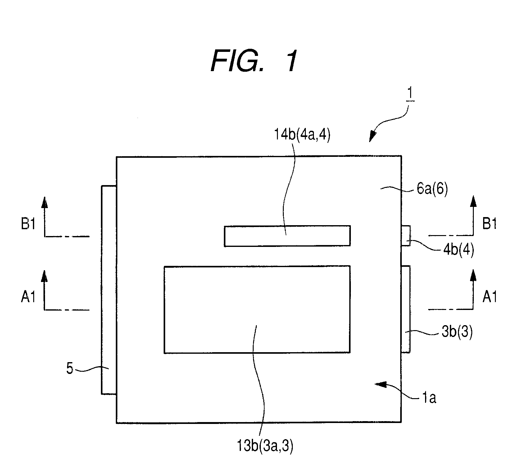
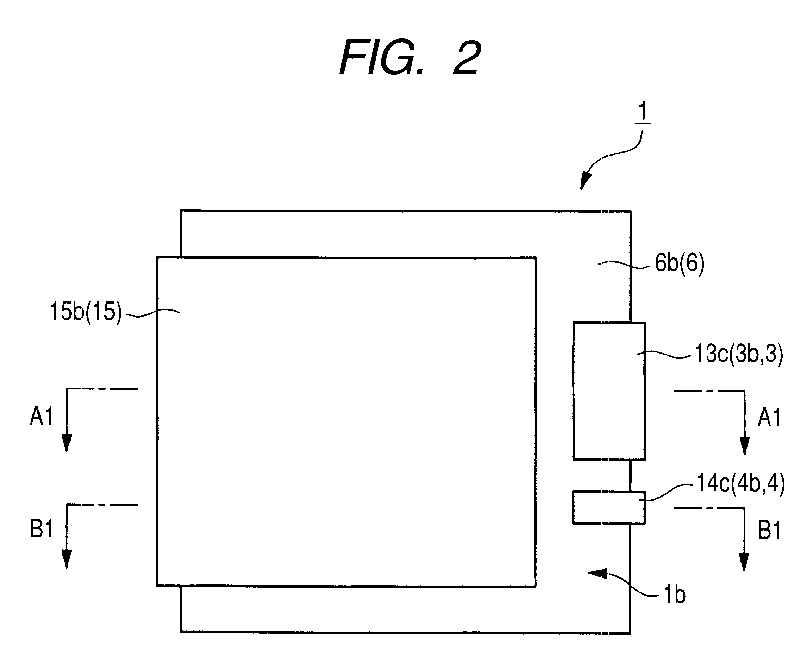
[0123]FIG. 1 is a top view (plan view) of the semiconductor device 1 as an embodiment of the invention; FIG. 2 is a bottom view (base view, back side view, plan view) thereof; and FIG. 3 and FIG. 4 are sectional views (side surface sectional views) thereof. A section taken along line A1-A1 of FIG. 1 (that is, a section taken along line A1-A1 of FIG. 2) substantially corresponds to FIG. 3; and a section taken along line B1-B1 of FIG. 1 (that is, a section taken along line B1-B1 of FIG. 2) substantially corresponds to FIG. 4.

[0124]The semiconductor device (semiconductor package) 1 in this embodiment is a resin sealed and surface mounted semiconductor package. That is, the semiconductor device 1 is a semiconductor device of a resin sealed semiconductor package type.

[0125]The semiconductor device 1 in this embodiment, illustrated in FIG. 1 to FIG. 4, includes: a semiconductor chip 2; ...

second embodiment

[0234]In the first embodiment, variation in the height h1 of the assembly 40 immediately before the molding step is suppressed by taking the following measure: not only the bonding materials 7a, 7b (7) but also the film members 8a, 8b are placed between the semiconductor chip 2 and the terminals. In the second embodiment, variation in the height h1 of the assembly immediately before the molding step is suppressed without use of the film member 8a or 8b. This is done by giving a twist to the type of the bonding materials 7a, 7b and the curing step for the bonding materials 7a, 7b.

[0235]FIG. 29 is a process flowchart illustrating the manufacturing process for the semiconductor device 1c in this embodiment. FIG. 30, FIG. 31, and FIG. 34 to FIG. 37 are substantial part sectional views illustrating the manufacturing process for the semiconductor device 1c in this embodiment. Of these drawings, FIG. 30 and FIG. 31 are different sectional views illustrating an identical process step; FIG....

third embodiment

[0265]In the first embodiment, variation in the height h1 of the assembly 40 immediately before the molding step is suppressed by taking the following measure: not only the bonding materials 7a, 7b but also the film members 8a, 8b are placed between the semiconductor chip 2 and the terminals. In the second embodiment, variation in the height h1 of the assembly 40c immediately before the molding step is suppressed by taking the following measure: the silver paste 7c containing the spacer particles 66 is used and the silver paste 7c is cured while pressure (load) is applied thereto. In the third embodiment, meanwhile, a semiconductor device favorable in fabrication yield and excellent in heat radiation characteristic even though there is variation in the height of an assembly immediately before the molding step is provided.

[0266]FIG. 39 is a process flowchart illustrating the manufacturing process for the semiconductor device 1d in this embodiment. The drawings from FIG. 40 to FIG. 48...


PUM


Abstract

The radiation performance of a resin sealed semiconductor package is enhanced and further the fabrication yield thereof is enhanced. A drain terminal coupled to the back surface drain electrode of a semiconductor chip is exposed at the back surface of an encapsulation resin section. Part of the following portion and terminal is exposed at the top surface of the encapsulation resin section: the first portion of a source terminal coupled to the source pad electrode of the semiconductor chip and a gate terminal coupled to the gate pad electrode of the semiconductor chip. The remaining part of the second portion of the source terminal and the gate terminal is exposed at the back surface of the encapsulation resin section. When this semiconductor device is manufactured, bonding material and a film member are placed between the drain terminal and the semiconductor chip. At the same time, paste-like bonding material and a film member are placed between the source terminal 3 and gate terminal and the semiconductor chip. The paste-like bonding material is cured and turned into bonding material. As the result of use of the film members, variation in the thickness of the bonding material is suppressed.

Description

CROSS-REFERENCE TO RELATED APPLICATIONS[0001]The disclosure of Japanese Patent Application No. 2008-41765 filed on Feb. 22, 2008 including the specification, drawings and abstract is incorporated herein by reference in its entirety.BACKGROUND OF THE INVENTION[0002]The present invention relates to manufacturing methods of semiconductor devices and in particular to a technique effectively applicable to manufacturing techniques for semiconductor devices of a resin sealed semiconductor package type.[0003]Among various semiconductor packages in use, there are resin sealed semiconductor packages obtained by sealing a semiconductor chip with an encapsulation resin section. In the resin sealed semiconductor package, a semiconductor chip is sealed in an encapsulation resin section; therefore, the reliability of the semiconductor chip can be enhanced. When terminals are exposed at the back surface of the encapsulation resin section, the resin sealed semiconductor package can be surface mounte...

Claims


Application Information

Patent Timeline
Patent Type & Authority Applications(United States)
IPC IPC(8): H01L21/56
CPCH01L21/565H01L23/3107H01L23/433H01L23/4334H01L23/49537H01L23/49551H01L23/49562H01L23/49575H01L24/29H01L24/33H01L24/36H01L24/40H01L24/41H01L24/83H01L25/115H01L25/117H01L2224/27013H01L2224/2929H01L2224/29339H01L2224/32014H01L2224/4899H01L2224/83051H01L2224/83192H01L2224/83855H01L2924/01002H01L2924/01005H01L2924/01013H01L2924/01015H01L2924/01029H01L2924/01033H01L2924/01047H01L2924/01057H01L2924/01074H01L2924/01075H01L2924/01078H01L2924/01079H01L2924/01082H01L2924/0781H01L2924/14H01L2924/16195H01L2924/30107H01L2924/3011H01L2224/83139H01L24/48H01L2224/29499H01L2224/83101H01L2224/83815H01L2224/83862H01L2224/83885H01L2924/01006H01L2924/01019H01L2924/01067H01L2924/014H01L2924/0665H01L2924/10253H01L2224/29101H01L2224/32245H01L2924/1815H01L2224/73263H01L2224/40247H01L2224/26145H01L2224/26175H01L2224/33181H01L2225/1029H01L2924/1306H01L2924/00H01L2924/00014H01L2924/07025H01L2924/3512H01L2924/351H01L2924/181H01L2224/84801H01L2224/83801H01L2224/8385H01L2224/8485H01L2224/06181H01L2224/0603H01L2924/00012H01L2224/45099H01L2224/45015H01L2924/207H01L2224/37099H01L2224/37599H01L2224/73221
Inventor MUTO, AKIRAKOIKE, NOBUYAARAI, KATSUOFUJIKI, ATSUSHI
Owner RENESAS ELECTRONICS CORP
Why Eureka
Try Eureka