Method for making chip resistor components

a chip resistor and component technology, applied in resistor chip manufacturing, resistors adapted for terminal application, resistive material coating, etc., can solve the problem of relatively complex structure of the above-mentioned conventional resistor, and achieve the effect of simple and cost-effective chip resistor components

Active Publication Date: 2009-09-03
YAGEO CORP
View PDF2 Cites 16 Cited by
  • Summary
  • Abstract
  • Description
  • Claims
  • Application Information

AI Technical Summary

Benefits of technology

[0005]The object of the present invention is to provide a method for making chip resistor component that is simple and cost effective.

Problems solved by technology

The aforesaid conventional resistor has a relatively complex structure.

Method used


Image

  • Method for making chip resistor components
  • Method for making chip resistor components
  • Method for making chip resistor components

Examples


Embodiment Construction

[0029]FIG. 1 illustrates consecutive steps of the preferred embodiment of a method for making chip resistor components according to this invention.

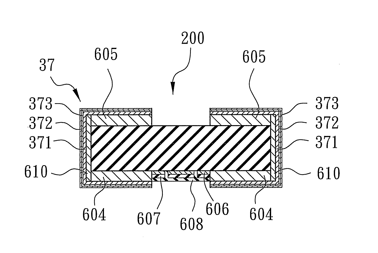
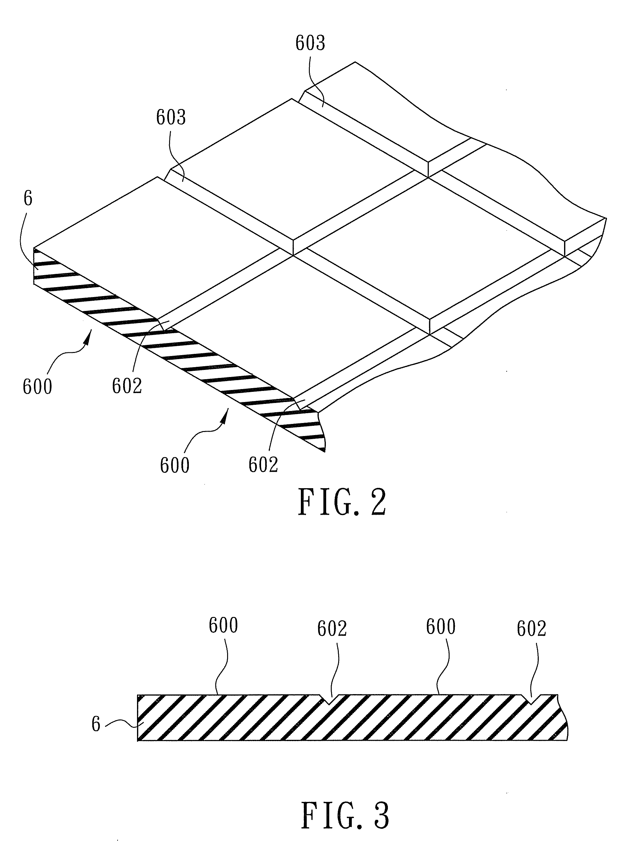
[0030]The method for making chip resistor components includes: (a) forming a plurality of intersecting strip-like first and second notches 602, 603 in a dielectric substrate 6 so as to form a plurality of resistor-forming strips 600 separated by the first notches 602 (see FIGS. 2 and 3); (b) forming a pair of spaced apart strip-like upper electrodes 605 on an upper surface of each of the resistor-forming strips 600, and a pair of spaced apart strip-like lower electrodes 604 on a lower surface of each of the resistor-forming strips 600, the upper and lower electrodes 605, 604 being substantially parallel to the first notches 602 (see FIGS. 4 and 5); (c) forming a strip-like resistor film 606 on the lower surface of each of the resistor-forming strips 600 such that the resistor film 606 extends between and is brought into contact with the l...


PUM

PropertyMeasurementUnit
structureaaaaaaaaaa
insulatingaaaaaaaaaa
resistanceaaaaaaaaaa

Abstract

A method for making chip resistor components includes: (a) forming a plurality of first and second notches in a substrate so as to form resistor-forming strips; (b) forming pairs of upper and lower electrodes on each of the resistor-forming strips; (c) forming a resistor film on each of the resistor-forming strips; (d) forming an insulator layer on the resistor film; (e) forming a hole pattern in the insulator layer and the resistor film; (f) forming an insulating shield layer on the insulator layer; (g) cleaving the substrate along the first notches so as to form a plurality of strip-like semi-finished products; (h) forming a pair of side electrodes on two opposite sides of each of the semi-finished products; and (i) cleaving each of the semi-finished products.

Description

BACKGROUND OF THE INVENTION[0001]1. Field of the Invention[0002]This invention relates to a method for making chip resistor components.[0003]2. Description of the Related Art[0004]U.S. Patent Application Publication No. 2003 / 0156008 discloses a resistor including a substrate, a pair of upper electrode layers formed on an upper surface of the substrate, a resistor layer formed on the upper surface of the substrate and connected to the upper electrode layers, a protective layer covering the resistor layer, a pair of L-shaped first side electrode layers formed on two sides and end portions of a lower surface of the substrate and contacting the respective upper electrode layer, a pair of L-shaped second side electrode layers covering respectively the first side electrode layer, a pair U-shaped first plating layers covering respectively the second side electrode layers and the upper electrode layers, and a pair of U-shaped second plating layers covering respectively the first plating lay...

Claims


Application Information

Patent Timeline
Patent Type & Authority Applications(United States)
IPC IPC(8): H01C17/06
CPCH01C17/006H01C17/06Y10T29/49099Y10T29/49101Y10T29/49082Y10T29/49124
Inventor CHEN, MU-YUANWU, WEN-FENGCHANG, CHI-PINCHIEN, KAO-PO
Owner YAGEO CORP
Why Eureka
Try Eureka