Tamper-proof caps for large assembly

a technology for tamper-proof caps and large assemblies, applied in the field of electronic packages, can solve the problems of limited current solution, difficult work, and high production cost of tamper-proof systems described above, and achieve the effect of simple and cost-effectiv

Inactive Publication Date: 2007-02-15
IBM CORP
View PDF4 Cites 96 Cited by
  • Summary
  • Abstract
  • Description
  • Claims
  • Application Information

AI Technical Summary

Benefits of technology

[0018] It is still a further object of the invention to provide a simple and cost-effective method of building tamper-proof layers and caps within PCB substrate for secure cryptographic applications.

Problems solved by technology

They are also made difficult to work with, for example due to intrinsic material / layer fragility when tampered (very low thickness, brittle layers, not solderable) such as to prevent shunting of the electrical circuit.
The tamper-proof systems as described above are efficient but are expensive and cumbersome to produce.
False calls during the manufacturing operations and in the field show the limits of the current solution.
Furthermore, such solution presents several drawbacks such as:
One of higher concern is localized bowing that causes elongation and eventually failure of the highly resistive tracks of the secure mesh triggering a tamper-sensing.
As all the plastic electronic packages using plastic polymer sealing that is not moisture proof, moisture is absorbed by the polymer in time, and gets desorbed with thermal cycles.
The polymer film with exposed resistive traces show limits during handling and the gift-wrapping of the box.
The resulting lines abrasion breaks the resistive network.

Method used


Image

  • Tamper-proof caps for large assembly
  • Tamper-proof caps for large assembly
  • Tamper-proof caps for large assembly

Examples


Embodiment Construction

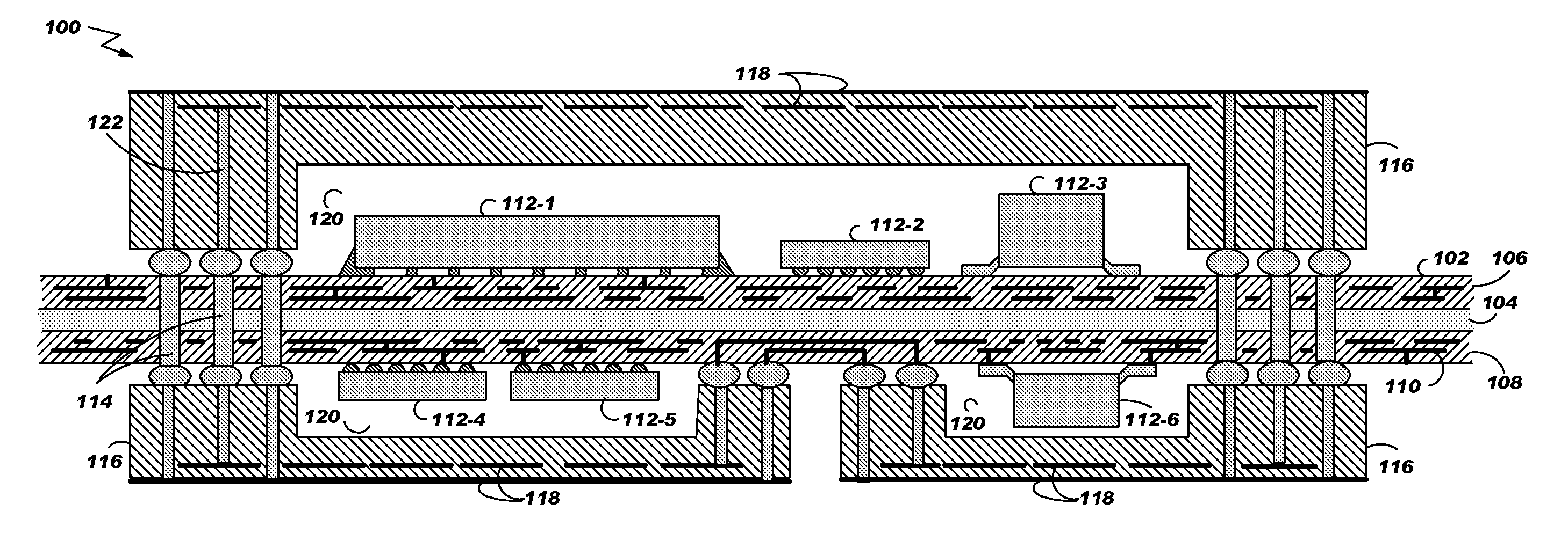
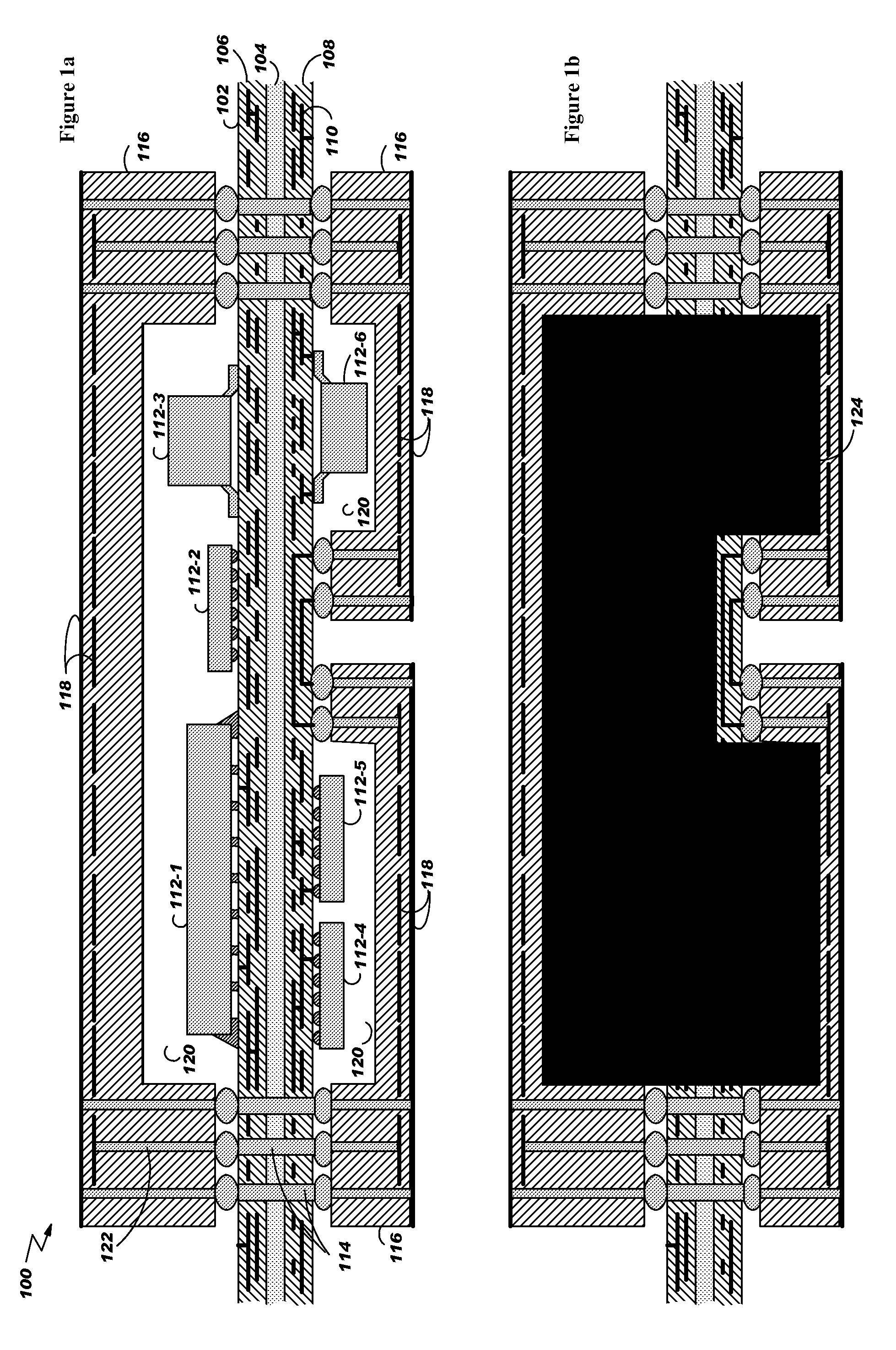
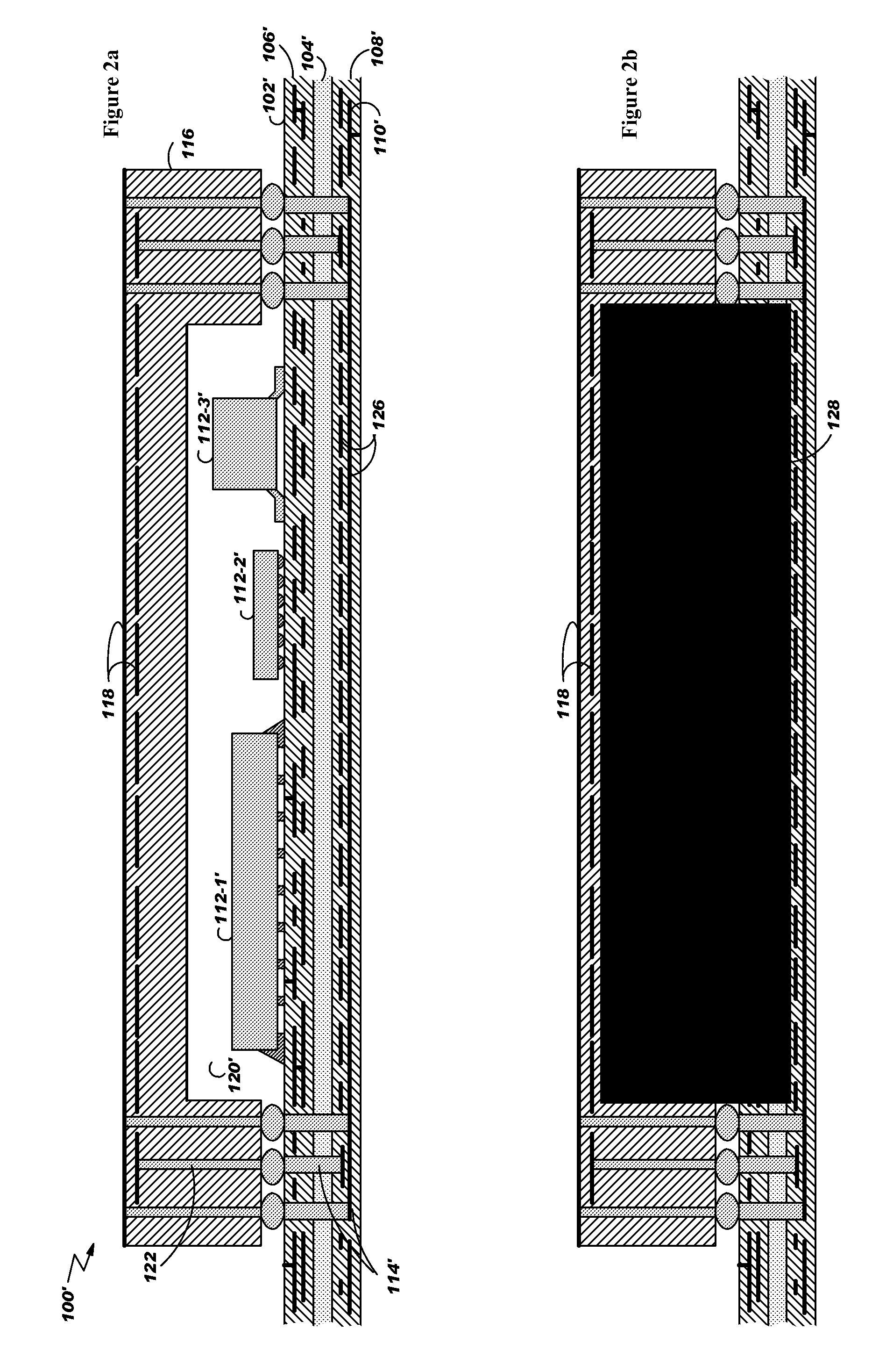
[0038] According to the invention tamper-proof caps are used to cover the parts of a Printed Circuit Board (PCB) that need to be protected. In the simplest case, a single cap is used to protect the whole part of the PCB that must be protected. In other cases, several caps can be used, possibly on each side of the PCB. In a further embodiment, passive or active electronic devices can be embedded within the tamper-proof caps. The multi-cap solution offers relief from the thermal point of view splitting, under different caps, the different high dissipation comps. In the same time with different sizes caps there is the possibility to expand and or change the components used in the application allowing upgrades in performance and functions.

[0039] Tamper-Proof Caps

[0040]FIG. 1, comprising FIGS. 1a and 1b, illustrates an example of the system 100 of the invention. For sake of illustration, caps are mounted on both sides of the PCB, one side of the PCB being protected by two caps. As show...


PUM

PropertyMeasurementUnit
viscosityaaaaaaaaaa
viscosityaaaaaaaaaa
viscosityaaaaaaaaaa

Abstract

A tamper-proof cap adapted to be mounted on a large assembly for shielding a selected area of the large assembly is disclosed. The tamper-proof cap comprises a laminate stack-up structure wherein at least one open chamber is formed. The stack-up structure comprises at least two layers wherein tamper-proof layers are formed on top of the open chamber. A plurality of vias are disposed around the open chamber, forming with said tamper proof layers a tamper-proof structure around said open chamber. The vias are adapted for connecting the tamper-proof layers to the large assembly when the tamper-proof cap is mounted. In a preferred embodiment, the tamper-proof cap further comprises a shielding layer on top of the tamper-proof layer that are preferably done using conductive ink.

Description

FIELD OF THE INVENTION [0001] The present invention relates generally to electronic packages and to secure electronic packages and more specifically to tamper-proof caps for large assembly. BACKGROUND OF THE INVENTION [0002] According to the Department of Commerce of the United States of America, all secure cryptographic application are classified according to one of four possible levels listed in the technical specification untitled “Security requirements for cryptographic modules” published in the Federal Information Processing Standards FIPS PUB 140-2 by the National Institute of Standards and Technology (NIST). This standard specifies the security requirements that must be satisfied by a cryptographic module to be utilized within a security system, protecting sensitive but unclassified information. The standard provides four increasing qualitative levels of security that are intended to cover a wide range of potential applications and environments in which cryptographic modules ...

Claims


Application Information

Patent Timeline
Patent Type & Authority Applications(United States)
IPC IPC(8): H04L9/00
CPCG06F21/87Y10T29/49165H05K1/141H05K2201/0715H05K2201/10151H01L23/576H01L2224/16225H01L2924/15156H01L2924/3025Y10T29/49128Y10T29/4913Y10T29/49174Y10T29/49172Y10T29/49126H05K1/0275
Inventor OGGIONI, STEFANO SERGIOCONDORELLI, VINCENZOHADZIC, NIHAD
Owner IBM CORP
Why Eureka
Try Eureka