Method of manufacturing a display

a display and manufacturing method technology, applied in the field of manufacturing a display, can solve the problems of affecting the visibility of a displayed image, affecting the effect of display quality, so as to keep the equipment cost necessary and short time without trapping air bubbles

Active Publication Date: 2009-09-03
PANASONIC LIQUID CRYSTAL DISPLAY CO LTD +1
View PDF7 Cites 30 Cited by
  • Summary
  • Abstract
  • Description
  • Claims
  • Application Information

AI Technical Summary

Benefits of technology

[0032]The present invention relates to a method of bonding a transparent interlayer whose refractive index is the same as, or close to, that of the above-mentioned display panel and the protective plate for protecting the display panel between the display panel and the protective plate without trapping air bubbles or the like. An object of the present invention is to provide a display manufacturing method that is less limited in terms of employable materials, that can keep the equipment cost necessary for the manufacture low, and that is capable of forming a transparent interlayer between a display panel and a protective plate in a short time without trapping air bubbles.
[0042]A manufacturing method according to the present invention is less limited in terms of the physical properties of materials that can be used as a transparent interlayer, and can keep the equipment cost necessary for the manufacture low. Further, a transparent interlayer can be formed in a short time without trapping air bubbles between a display panel and a protective plate.

Problems solved by technology

In personal computer monitors, home-use televisions, and other similar appliances, too, where the liquid crystal panel surface is touched less frequently, the liquid crystal panel itself could be shattered if something like tableware or a toy hits the liquid crystal panel surface with a large enough force.
However, putting a transparent protective plate in front of a liquid crystal panel causes reflection of light at the interface between materials having different optical characteristics, specifically, refractive indices.
At these interfaces, it is observed that the difference in refractive index between materials causes the reflection of light, which significantly impairs the visibility of a displayed image especially in a bright environment.
A problem of using a thermoplastic resin interlayer made of the PVB resin in this manufacturing method is that the interlayer needs to be bonded at high temperature and high pressure in an autoclave after temporary thermal bonding, which is laborious.
Other problems include costly plant and equipment investment due to the installation of an autoclave, and poor production efficiency since the main press-fit using an autoclave is a batch process.
However, the method of bonding a sheet-shaped transparent interlayer in vacuum has a problem in that the need to use an autoclave for a high-temperature, high-pressure process in order to obtain sufficient adhesion without trapping air bubbles makes the work laborious.
Other problems of this method include costly plant and equipment investment due to the installation of an autoclave and poor production efficiency since the main press-fit using an autoclave is a batch process.
Although methods capable of laminating glass at room temperature without needing temporary thermal bonding and a high-temperature, high-pressure process that uses an autoclave have been published in order to solve the above-mentioned problems of vacuum bonding, these methods do not require temporary thermal bonding and a high-temperature, high-pressure process that uses an autoclave by adjusting the physical properties and the like of the interlayer bonded between two glass plates, and are therefore limited in terms of materials that can be employed in order to eliminate the necessity of performing temporary thermal bonding and a high-temperature, high-pressure process that uses an autoclave.
This method, however, involves an injection length of the interlayer resin and has a fear of trapping air bubbles.

Method used


Image

  • Method of manufacturing a display
  • Method of manufacturing a display
  • Method of manufacturing a display

Examples


first embodiment

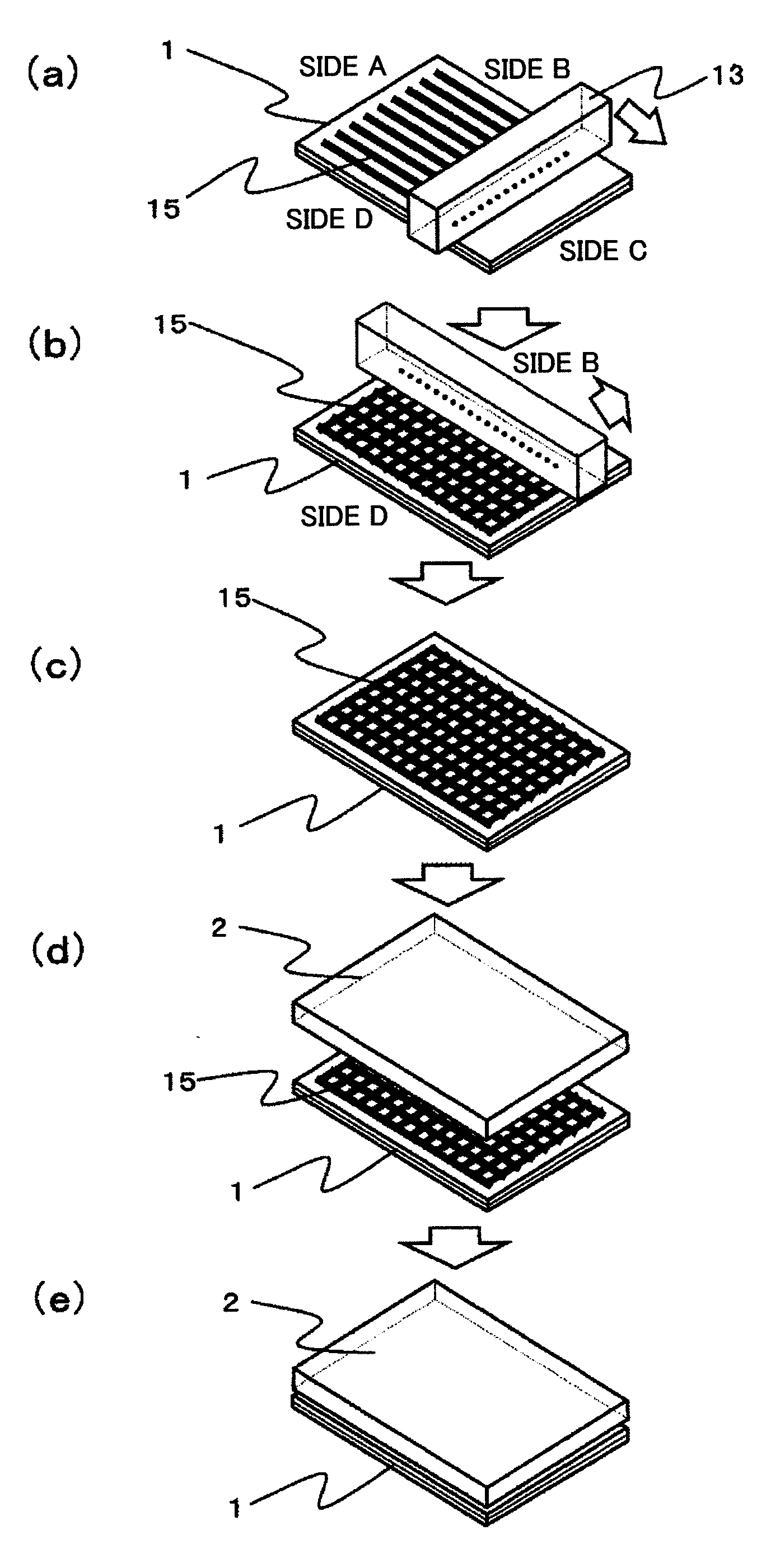
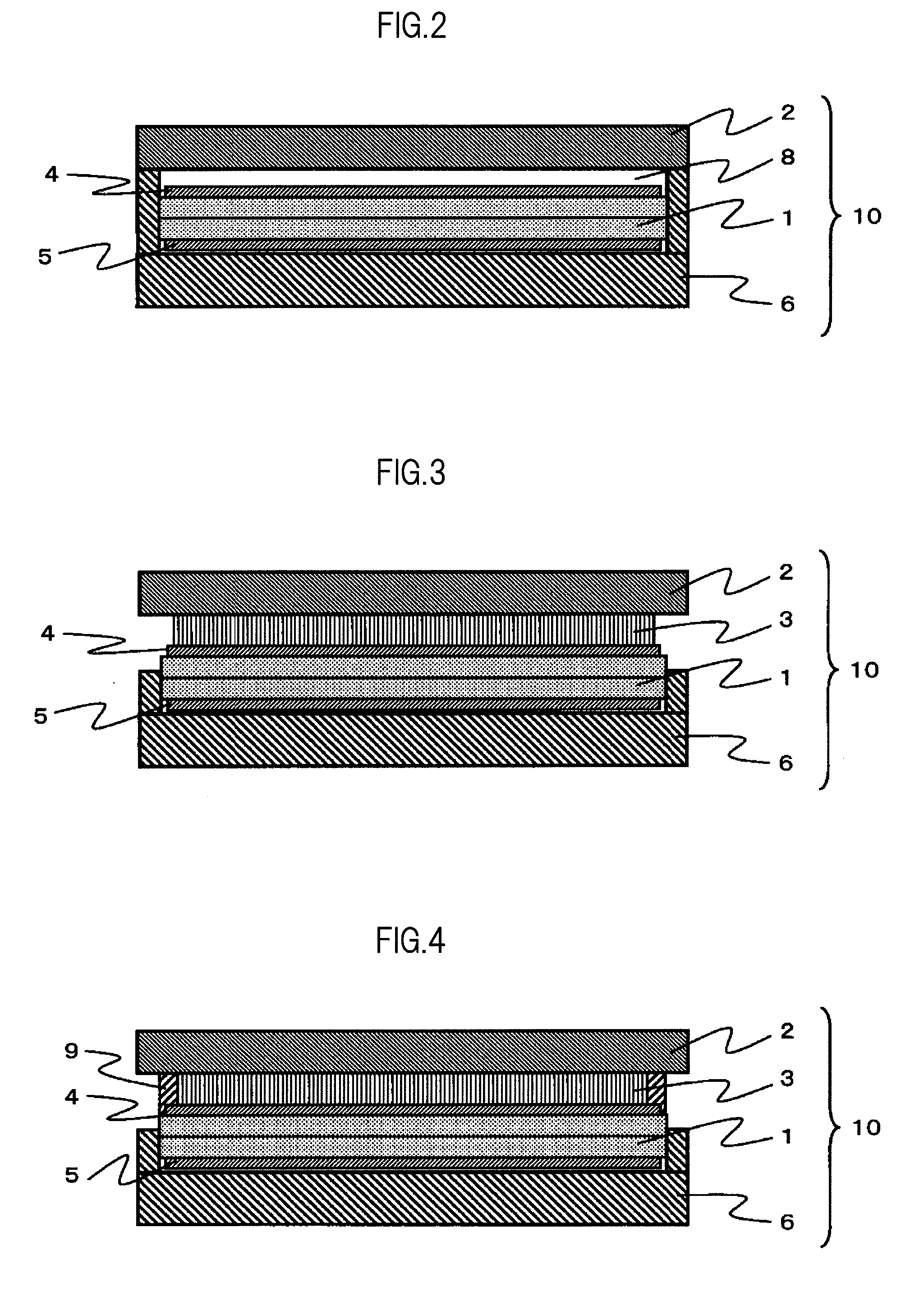
[0204]A first embodiment of the present invention is described with reference to FIGS. 1A to 1E. First, the multi-application nozzle 13 is used to apply the liquid organic medium 15 to a surface of the liquid crystal display panel 1 from Side A to Side C (or from Side C to Side A; either way, the direction does not matter) in a stripe pattern (FIG. 1A). Next, the liquid organic medium 15 is applied to the same surface of the liquid crystal display panel 1 from Side D to Side B (or from Side B to Side D; either way, the direction does not matter) in a stripe pattern that intersects the previously formed stripe application pattern (FIG. 1B). A grid pattern illustrated in FIG. 1C is thus formed. Although FIGS. 1A to 1C illustrate a method of using the multi-application nozzle 13 to form a grid-like application pattern, the grid-like application pattern may be formed by screen printing or offset printing as described in [Liquid Organic Medium Application Methods].

[0205]Next, the protect...

second embodiment

[0207]A second embodiment of the present invention is described with reference to FIGS. 6A to 6F. First, the multi-application nozzle 13 is used to apply the liquid organic medium 15 to a surface of the liquid crystal display panel 1 from Side A to Side C (or from Side C to Side A; either way, the direction does not matter) in a stripe pattern (FIGS. 6A and 6B). Next, the multi-application nozzle 13 is used to apply the liquid organic medium 15 to a surface of the protective plate 2 from Side D to Side B (or from Side B to Side D; either way, the direction does not matter) in a stripe pattern (FIGS. 6C and 6D). Although FIGS. 6A to 6D illustrate a method of using the multi-application nozzle 13 to form a stripe application pattern, the stripe application pattern may be formed by screen printing or offset printing as described in [Liquid Organic Medium Application Methods].

[0208]Next, the protective plate 2, where the liquid organic medium 15 has been formed in a stripe pattern, is p...

third embodiment

[0210]A third embodiment of the present invention is described with reference to FIG. 7. First, a slit application nozzle 14 is used to apply the liquid organic medium 15 solidly to a surface of the liquid crystal display panel 1 from Side D to Side B (or from Side B to Side D, from Side A to Side C, from Side C to Side A; any way, the direction does not matter) (FIGS. 7A and 7B).

[0211]Next, the multi-application nozzle 13 is used to apply the liquid organic medium 15 to a surface of the protective plate 2 from Side A to Side C (or from Side C to Side A; either way, the direction does not matter) in a stripe pattern (FIG. 7C). The liquid organic medium 15 is then applied to the same surf ace of the protective plate 2 from Side D to Side B (or from Side B to Side D; either way, the direction does not matter) in a stripe pattern that intersects the previously formed stripe application pattern (FIG. 7D). A grid pattern illustrated in FIG. 7E is thus formed.

[0212]Thereafter, the protect...


PUM

PropertyMeasurementUnit
refractive indexaaaaaaaaaa
widthaaaaaaaaaa
thicknessaaaaaaaaaa

Abstract

In a method of manufacturing a display having a display panel, a transparent protective plate, which is placed in front of the display panel, and a layer formed of a transparent organic medium, which is placed between the display panel and the protective plate, a liquid organic medium is applied to, or a sheet-like organic medium is formed on, a surface of one of the display panel and the protective plate, the display panel and the protective plate are bonded together in a reduced pressure atmosphere, and thereafter the liquid organic medium is cured.

Description

CROSS-REFERENCE TO RELATED APPLICATION[0001]The present application claims priority from Japanese application JP2008-049403 filed on Feb. 29, 2008, the content of which is hereby incorporated by reference into this application.BACKGROUND OF THE INVENTION[0002]1. Field of the Invention[0003]The present invention relates to a method of manufacturing a display that has a transparent protective plate on a surface of a display panel, and more particularly, to a display manufacturing method in which a transparent organic medium layer is formed between the protective plate and the display panel.[0004]2. Description of the Related Art[0005]Many of displays for home-use televisions and personal computers and information displays installed in public facilities are liquid crystal displays or organic electroluminescence displays. Liquid crystal displays are employed in a particularly wide range of products from as small ones as 2-inch monitors for cellular phones and the like to 60-inch or larg...

Claims


Application Information

Patent Timeline
Patent Type & Authority Applications(United States)
IPC IPC(8): B32B17/04
CPCG02F2202/023G02F1/133502
Inventor KAWABE, SHINICHI
Owner PANASONIC LIQUID CRYSTAL DISPLAY CO LTD
Why Eureka
Try Eureka