Dual Channel Memory Architecture Having a Reduced Interface Pin Requirements Using a Double Data Rate Scheme for the Address/Control Signals

a dual-channel memory and address/control signal technology, applied in the field of memory architectures, can solve the problems of more complex packaging and circuit board design, design challenges, and the complexity of conventional memory interfaces using dual-channel circuits

Active Publication Date: 2009-09-03
QUALCOMM INC
View PDF5 Cites 48 Cited by
  • Summary
  • Abstract
  • Description
  • Claims
  • Application Information

AI Technical Summary

Benefits of technology

[0008]In yet another embodiment, a memory architecture may include a memory controller, a first memory device coupled to the memory controller by a shared control bus and a first clock signal, and a second memory device coupled to the memory controller by the shared control bus and a second clock signal, wherein the polarity of the second clock signal is opposite of the polarity of the first clock signal.
[000

Problems solved by technology

However, upgrading an existing processing system having a single data channel memory interface to one having dual memory interface may present some design challenges.
For example, conventional memory interfaces using dual channels may have more complex circuitry associated with the addressing and/or control channels.
This can

Method used


Image

  • Dual Channel Memory Architecture Having a Reduced Interface Pin Requirements Using a Double Data Rate Scheme for the Address/Control Signals
  • Dual Channel Memory Architecture Having a Reduced Interface Pin Requirements Using a Double Data Rate Scheme for the Address/Control Signals
  • Dual Channel Memory Architecture Having a Reduced Interface Pin Requirements Using a Double Data Rate Scheme for the Address/Control Signals

Examples


Embodiment Construction

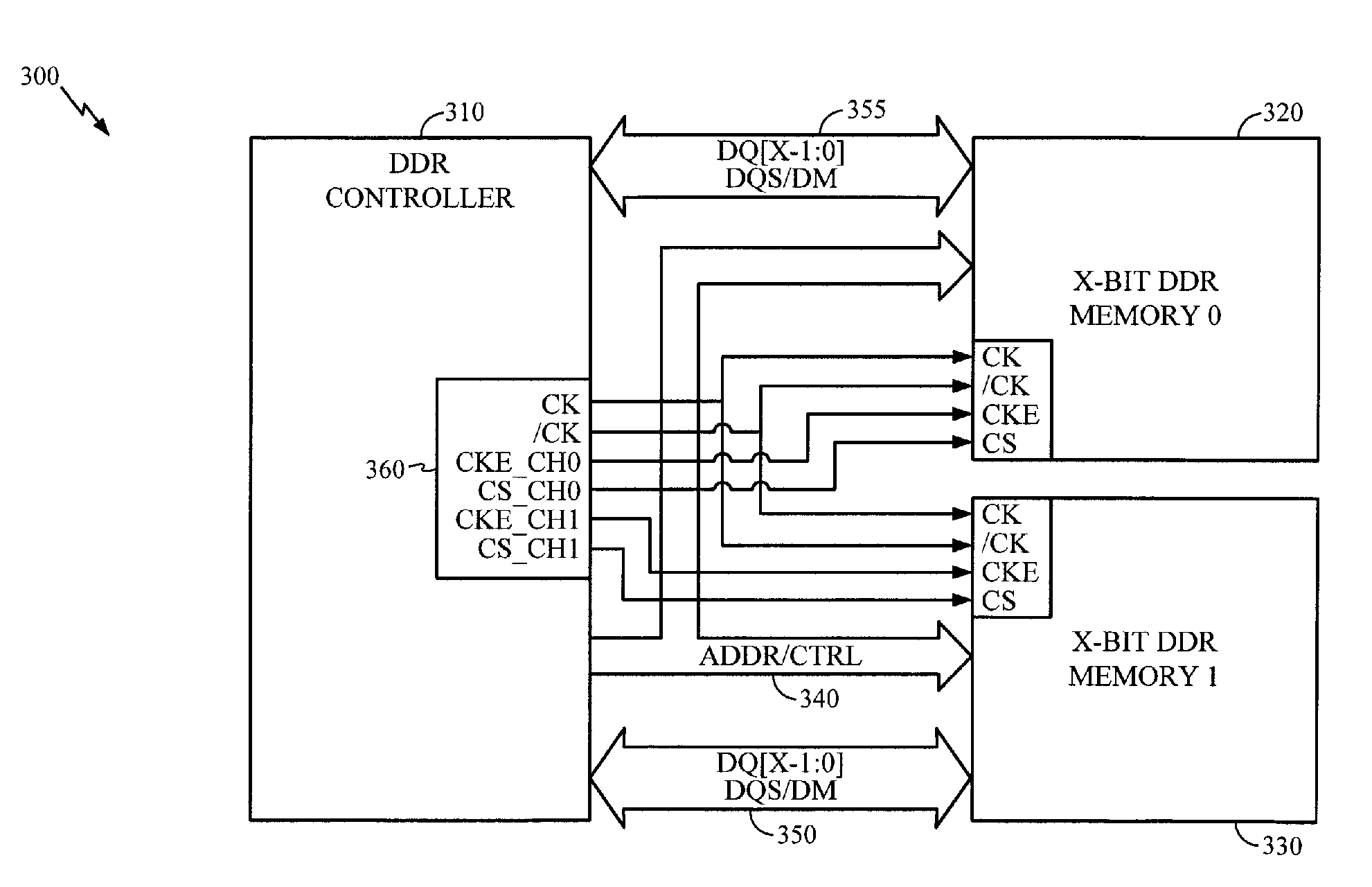
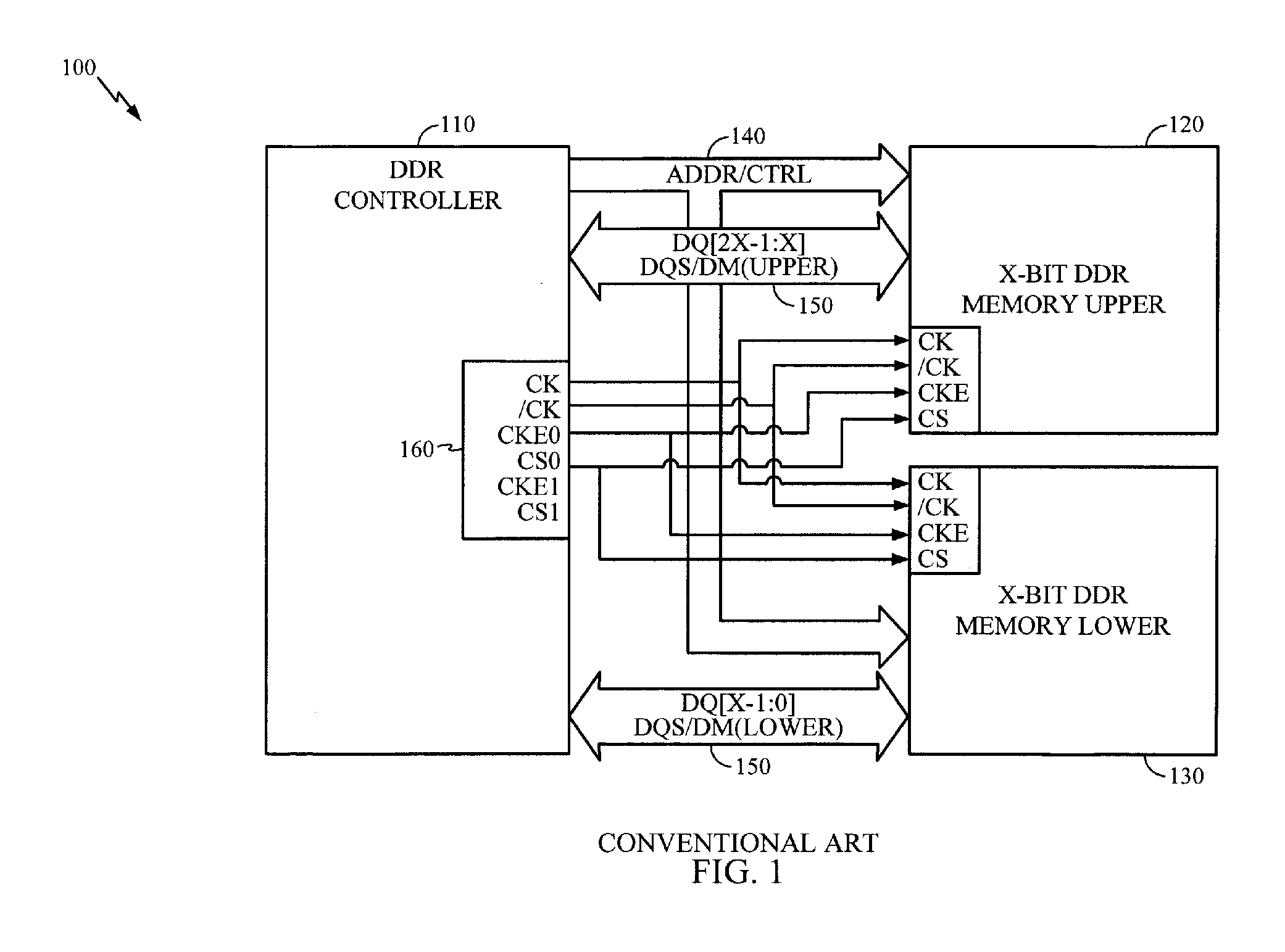
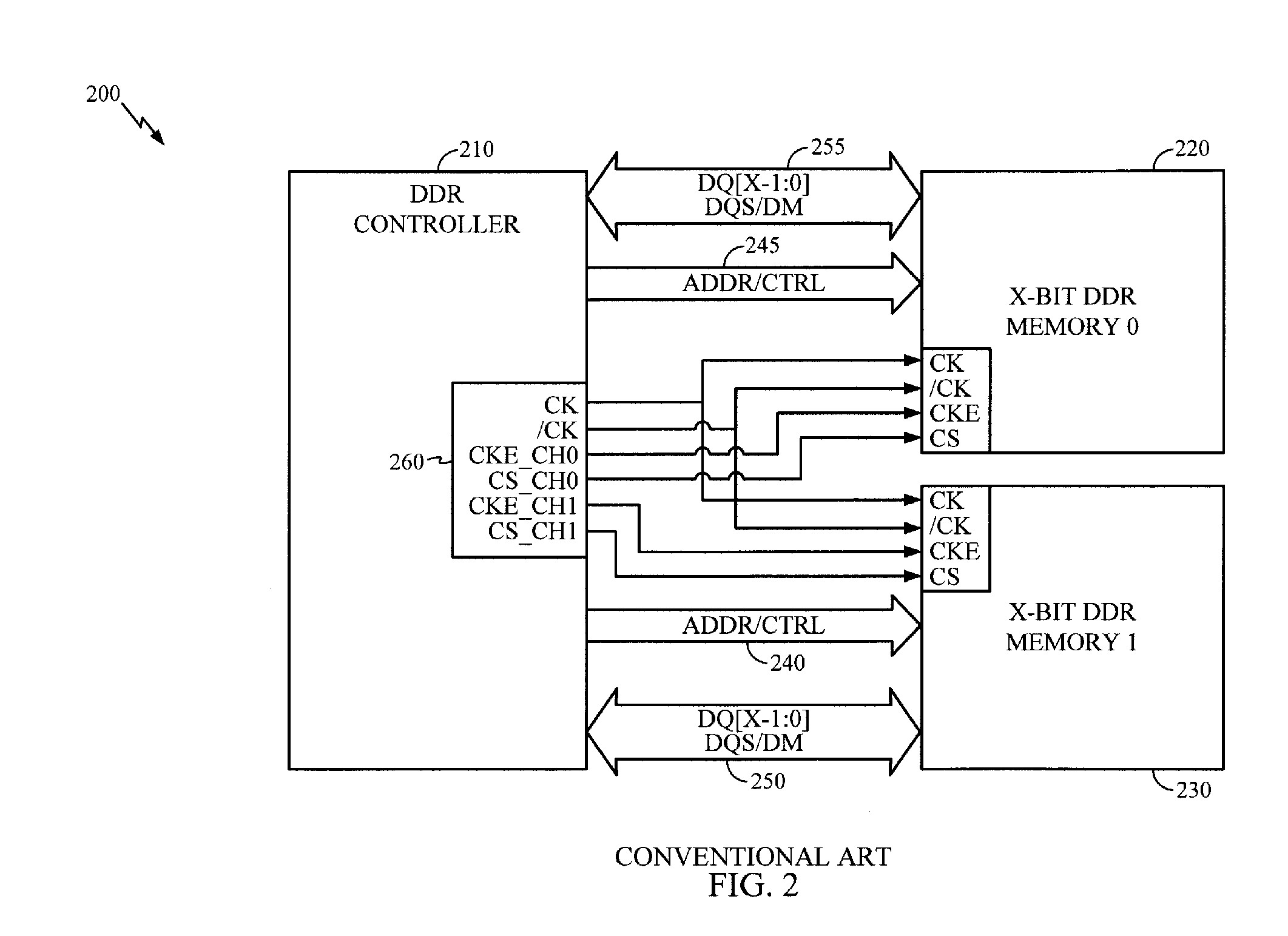
[0017]Aspects of the invention are disclosed in the following description and related drawings directed to specific embodiments of the invention. Alternate embodiments may be devised without departing from the scope of the invention. Additionally, well-known elements of the invention will not be described in detail or will be omitted so as not to obscure the relevant details of the invention.

[0018]The word “exemplary” is used herein to mean “serving as an example, instance, or illustration.” Any embodiment described herein as “exemplary” is not necessarily to be construed as preferred or advantageous over other embodiments. Likewise, the term “embodiments of the invention” does not require that all embodiments of the invention include the discussed feature, advantage or mode of operation.

[0019]The terminology used herein is for the purpose of describing particular embodiments only and is not intended to be limiting of embodiments of the invention. As used herein, the singular forms ...


PUM


Abstract

Apparatuses and methods for dual channel memory architecture with reduced interface pin requirements are presented. One memory architecture includes a memory controller, a first memory device coupled to the memory controller by a shared address bus and a first clock signal, and a second memory device coupled to the memory controller by the shared address bus and a second clock signal, where the polarity of the second clock signal is opposite of the first clock signal. A method for performing data transactions is presented. The method includes providing addressing signals over a shared address bus to a first memory device and a second memory device, providing clock signals to the memory devices which are reversed in polarity, where the clock signals are derived from a common clock signal, and transferring data to the memory devices over separate narrow data buses in an alternating manner based upon the clock signals.

Description

FIELD OF DISCLOSURE[0001]The embodiments of the disclosure relate generally to memory architectures, and more specifically, to dual data channel memory architecture circuits having reduced interface pin requirements.BACKGROUND[0002]In some applications, processors may have a large percentage of memory access operations which transfer small amounts of data. Such memory access operations may be commonly known as burst length access (e.g., burst length reads and / or burst length writes). Current research suggests that for small burst length access, multiple narrow independent data channels accessing the memory devices may provide better performance than a single data channel having a wide memory interface. Accordingly, existing systems having single, wide-channel memory interface could benefit by increasing the number of data channels while reducing each data channel's bit width.[0003]However, upgrading an existing processing system having a single data channel memory interface to one h...

Claims


Application Information

Patent Timeline
IPC IPC(8): G11C8/18
CPCG06F13/1684G06F13/1689Y02B60/1235Y02B60/1228G06F13/4243Y02D10/00
Inventor MAO, JIANSANKURATRI, RAGHU
Owner QUALCOMM INC
Why Eureka
Try Eureka