
Method of manufacturing wiring board and method of manufacturing semiconductor package

Active Publication Date: 2009-09-10
SHINKO ELECTRIC IND CO LTD
View PDF5 Cites 35 Cited by
  • Summary
  • Abstract
  • Description
  • Claims
  • Application Information

AI Technical Summary

Benefits of technology

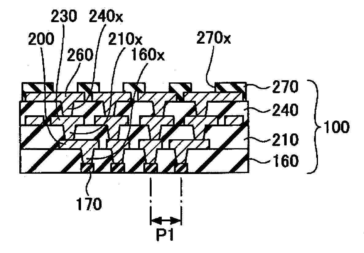
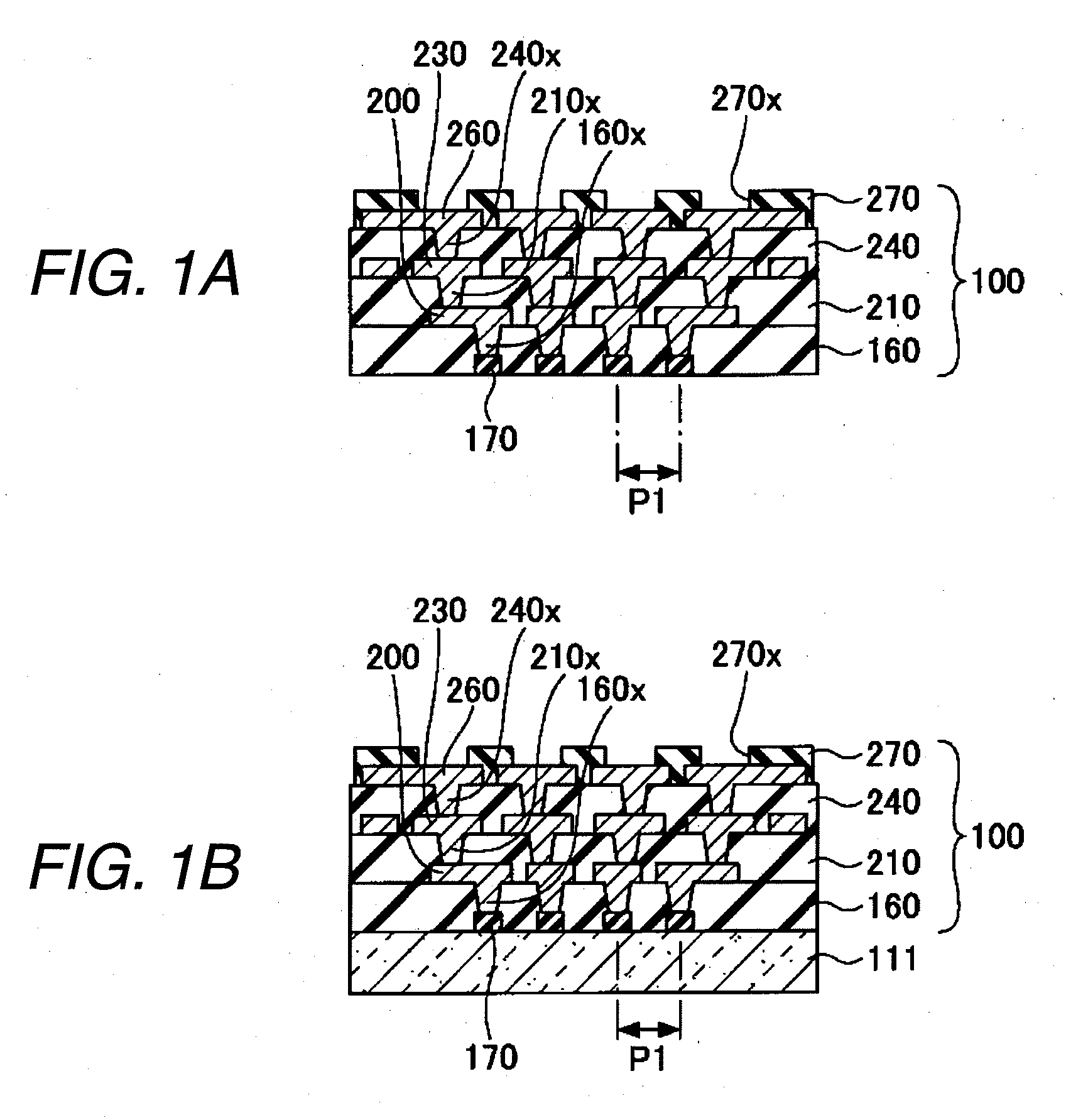
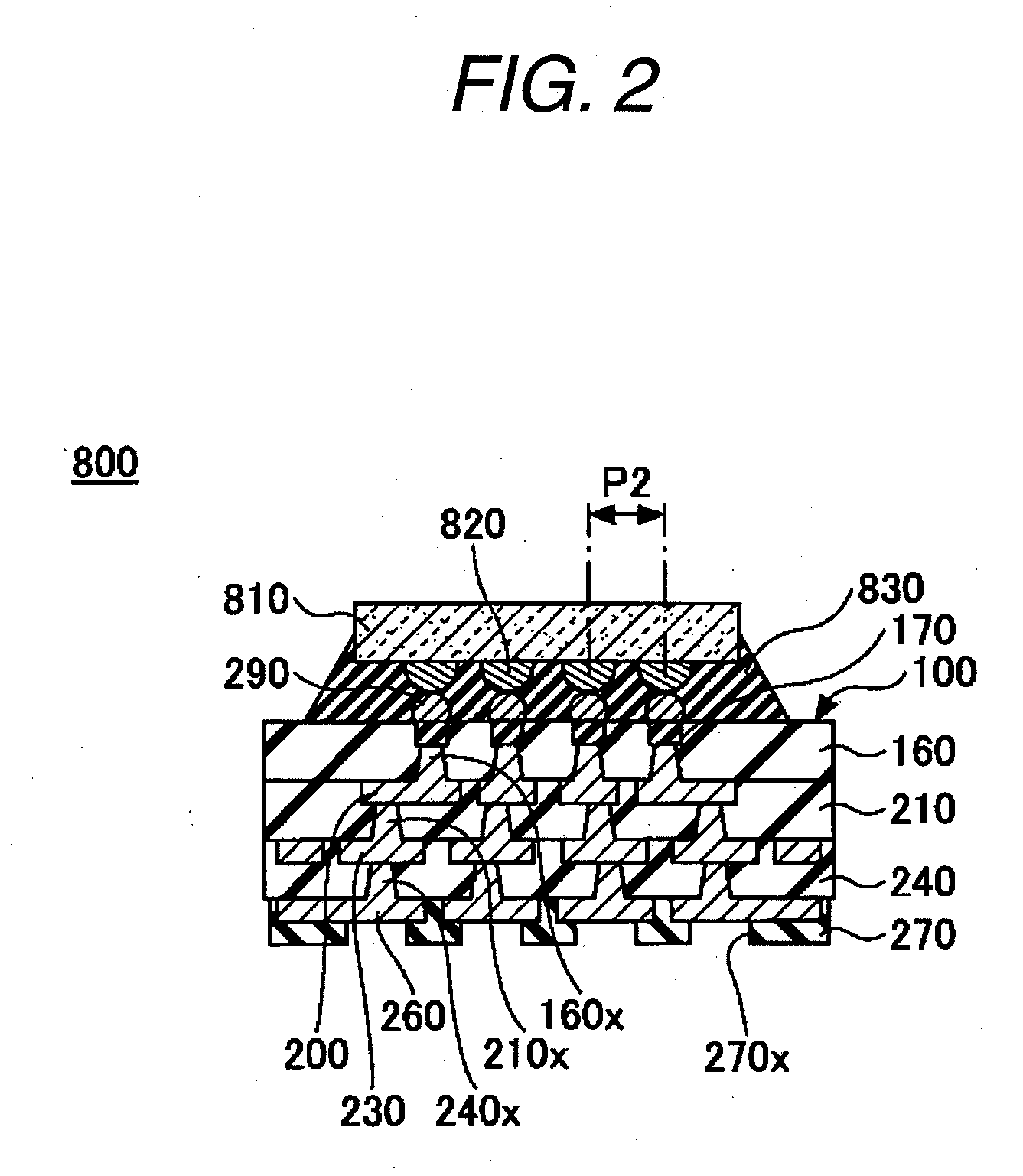
[0019]Exemplary embodiments of the present invention provide a method of manufacturing a wiring board which can reduce a shift, from a desirable pitch, of a pitch of an electrode pad to be electrically connected to a semiconductor chip and a method of manufacturing a semiconductor package which can reduce a shift of the pitch of the electrode pad of the wiring board from a pitch of an electrode of the semiconductor chip to be electrically connected to the electrode pad.
[0025]According to the invention, it is possible to provide a method of manufacturing a wiring board which can reduce a shift, from a desirable pitch, of a pitch of an electrode pad to be electrically connected to a semiconductor chip and a method of manufacturing a semiconductor package which can reduce a shift of the pitch of the electrode pad from a pitch of an electrode of the semiconductor chip to be electrically connected to the electrode pad.

Problems solved by technology

As a result, a warpage or a distortion is caused by a thermal stress due to a difference in the coefficient of thermal expansion between the wiring layer and the insulating layer.
For this reason, it is impossible to suppress a generation of the warpage or the distortion.
When a wiring board and a semiconductor chip, in which the pitches P1 and P2 are smaller than 100 μm and a solder bump and a ball-shaped terminal which are to correspond thereto also have sizes reduced, are to be electrically connected to each other, however, there is a problem in that it is hard to connect desirable portions to each other.

Method used


Image

  • Method of manufacturing wiring board and method of manufacturing semiconductor package
  • Method of manufacturing wiring board and method of manufacturing semiconductor package
  • Method of manufacturing wiring board and method of manufacturing semiconductor package

Examples


first embodiment

Variant of First Embodiment

[0123]In a variant of the first embodiment according to the invention, there will be shown a method of manufacturing the assembly wiring board 10 and the wiring board 10a having the buildup wiring layer which is different from that in the first embodiment according to the invention. In the variant of the first embodiment according to the invention, the concave portion 13 is not formed on the upper surface of the support board 11 but a first wiring layer 17 is formed on the upper surface of the support board 11 which is flat. Since materials and thicknesses of the support board 11 and the peeling layer 15 are the same as those in the first embodiment according to the invention, description thereof will be omitted.

[0124]FIGS. 25 to 27 are views illustrating a process for manufacturing the assembly wiring board 10 and the wiring board 10a according to the variant of the first embodiment in accordance with the invention. In FIGS. 25 to 27, the same components ...

second embodiment

[0131]In a second embodiment according to the invention, description will be given to a manufacturing method which is different from the method of manufacturing the assembly wiring board 10 and the wiring board 10a having the buildup wiring layer according to the first embodiment of the invention. An assembly wiring board and a wiring board which are manufactured by the method according to the second embodiment of the invention are set to be an assembly wiring board 30 and a wiring board 30a for convenience. Although the assembly wiring board 10 and wiring board 10a and the assembly wiring board 30 and wiring board 30a are manufactured by different methods from each other, they are identical to each other.

[0132]FIGS. 28 to 32 are views illustrating a process for manufacturing the assembly wiring board 30 and the wiring board 30a according to the second embodiment of the invention. In FIGS. 28 to 32, the same components as those in FIGS. 5 to 24 have the same reference numerals and d...

third embodiment

[0142]In a third embodiment according to the invention, description will be given to a manufacturing method which is different from the method of manufacturing the assembly wiring board 10 and the wiring board 10a having the buildup wiring layer according to the first embodiment of the invention. An assembly wiring board and a wiring board which are manufactured by the method according to the third embodiment of the invention are set to be an assembly wiring board 40 and a wiring board 40a for convenience. Although the assembly wiring board 10 and wiring board 10a and the assembly wiring board 40 and wiring board 40a are manufactured by different methods from each other, they are identical to each other.

[0143]FIGS. 33 to 35 are views illustrating a process for manufacturing the assembly wiring board 40 and the wiring board 40a according to the third embodiment of the invention. In FIGS. 33 to 35, the same components as those in FIGS. 5 to 24 have the same reference numerals and desc...


PUM


Abstract

A method of manufacturing a wiring board having a semiconductor chip mounting surface for mounting a semiconductor chip thereon which is manufactured by a process including a step of forming a wiring layer and an insulating layer on a support board and a step of removing the support board, including a peeling layer forming step of forming a peeling layer on the support board formed by a material having a coefficient of thermal expansion which is equal to that of a semiconductor substrate constituting the semiconductor chip, and a support board removing step of removing the support board by carrying out a predetermined treatment over the peeling layer.

Description

TECHNICAL FIELD[0001]The present disclosure relates to a method of manufacturing a wiring board and a method of manufacturing a semiconductor package. More particularly, the present disclosure relates to a method of manufacturing a wiring board having a semiconductor chip mounting surface mounting a semiconductor chip thereon, and a method of manufacturing a semiconductor package in which the semiconductor chip is mounted on the wiring board.RELATED ART[0002]For example, as a method of manufacturing a wiring board having a semiconductor chip mounting surface on which a semiconductor chip is to be mounted, there has been proposed a method of sequentially forming a predetermined wiring layer on a support board formed of Cu to form a buildup wiring layer and then removing the support board, thereby obtaining the wiring board.[0003]Referring to the wiring board manufacturing method of this type, the support board is present in the formation of the buildup wiring layer. Therefore, the bu...

Claims


Application Information

Patent Timeline
IPC IPC(8): H05K3/02
CPCH01L21/4857Y10T29/49144H01L21/6835H01L24/16H01L24/81H01L24/97H01L2221/68345H01L2224/81193H01L2224/81801H01L2224/97H01L2924/01029H01L2924/01046H01L2924/01074H01L2924/01078H01L2924/01079H01L2924/14H05K1/113H05K3/005H05K3/007H05K3/3473H05K3/4682H05K2201/0367H05K2201/068H05K2201/09527H05K2201/10674H05K2203/0108H05K2203/0113H05K2203/016H05K2203/0338H01L21/568Y10T29/49156Y10T29/49155Y10T29/4913Y10T29/49165H01L2224/73204H01L2924/01005H01L2924/01006H01L2924/01024H01L2924/01033H01L2224/16225H01L2224/32225H01L2224/81H01L2924/00H01L2924/351H01L2924/00012
Inventor MURAYAMA, KEIHIGASHI, MITSUTOSHISUNOHARA, MASAHIRO
Owner SHINKO ELECTRIC IND CO LTD
Learn More