

Semiconductor memory device and method of manufacturing thereof
a memory device and semiconductor technology, applied in semiconductor devices, capacitors, electrical devices, etc., can solve problems such as poor contact, oxidization of plugs, and process damage over ferroelectric capacitors to become larger
- Summary
- Abstract
- Description
- Claims
- Application Information
AI Technical Summary
Benefits of technology
Problems solved by technology
Method used
Image

Examples
first embodiment
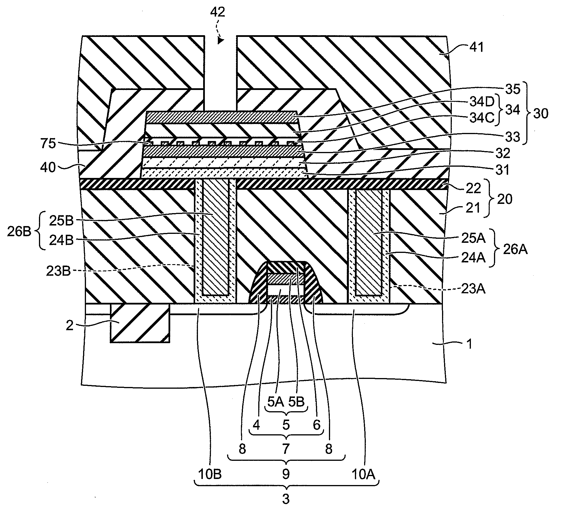
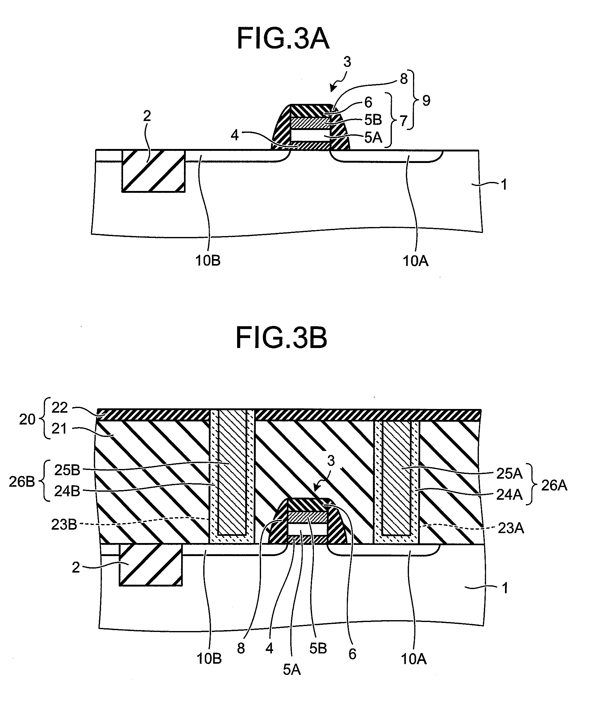
[0056]FIG. 1 is a partial sectional view schematically showing one example of a structure of a semiconductor memory device according to a first embodiment of the present invention. As shown in FIG. 1, in an upper surface of a semiconductor substrate 1, which is a p-type silicon substrate or the like, a field insulation film 2 formed with a silicon oxide film, etc. is formed. In an active region defined by the field insulation film 2, a MIS (metal-insulator-semiconductor) type electric field effect transistor (hereinafter to be referred to as MISFET) 3 with a structure of metal-insulator-semiconductor junction is formed. The MISFET 3 includes a gate structure 9, and source / drain regions 10A and 10B. The gate structure 9 is composed as including; a gate stack 7 in which a gate insulator 4, a gate electrode 5 which is to be a part of a word line, and a gate cap 6 are being laminated; and gate sidewall spacers 8 which are formed on both side surfaces of the gate stack 7 in a gate length...
second embodiment
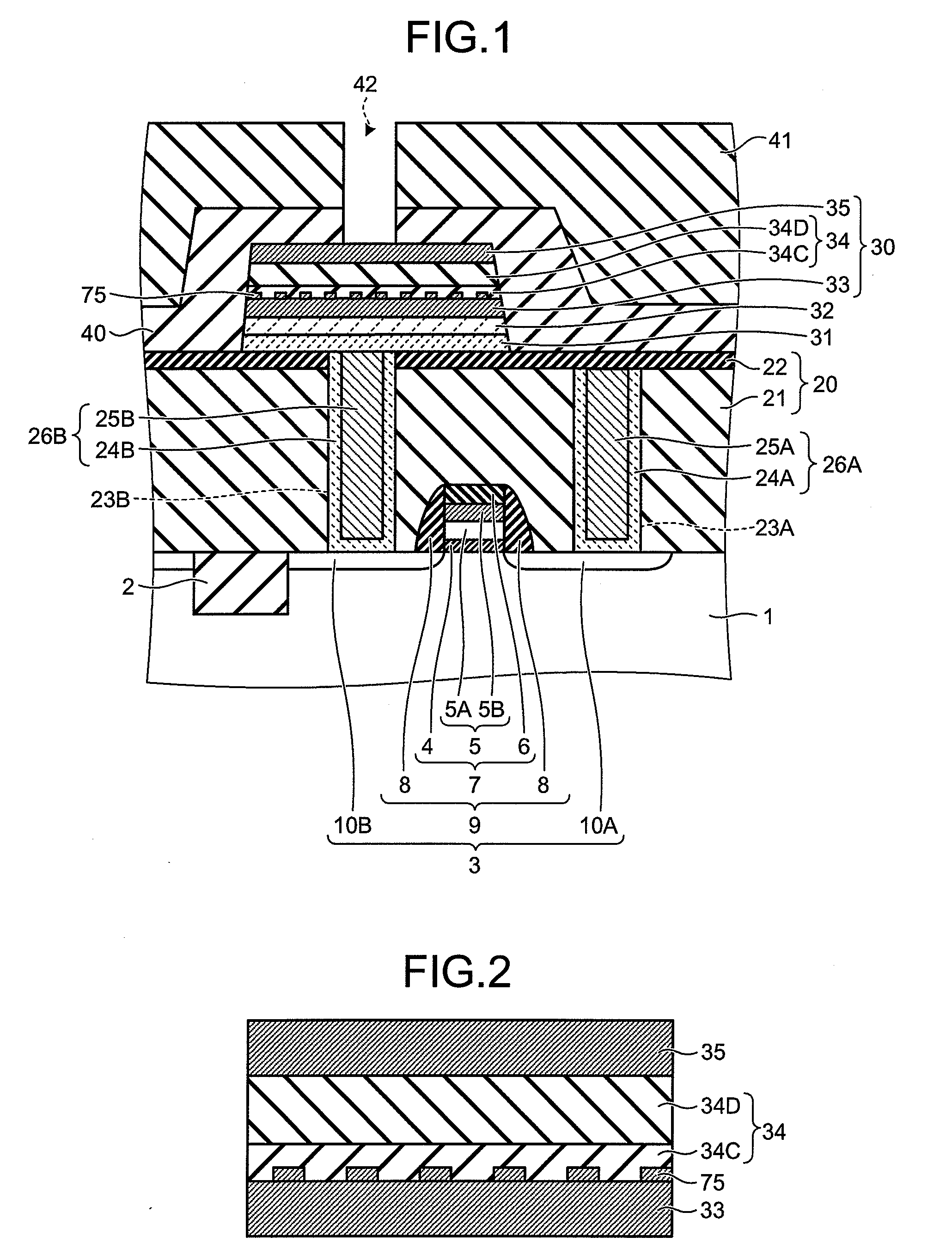
[0090]Now a semiconductor memory device and a method of manufacturing thereof according to a second embodiment of the present invention will be described. The second embodiment will refer to a case in which a concave-convex shape, which functions similarly to the nano-structures in the first embodiment, is formed on the surface of the lower electrode by processing the surface of the lower electrode.
[0091]FIG. 12 is a partial sectional view schematically showing one example of a structure of the semiconductor memory device according to the second embodiment of the present invention. In FIG. 12, parts of the structure other than a lower electrode 433 of the ferroelectric capacitor 30, the ferroelectric film 34, and the upper electrode 35 are similar to those in the structure shown in FIG. 1, and such parts therefore are not shown for brevity.
[0092]In the semiconductor memory device according to the second embodiment, convex portions 475 are formed on the surface of the lower electrode...
PUM
 Abstract
Description
Claims
Application Information