Protection for Bonding Pads and Methods of Formation

a technology of bonding pads and protective layers, which is applied in the direction of semiconductor devices, semiconductor/solid-state device details, electrical devices, etc., can solve the problems of metal materials such as copper exposed to air or other unprotected ambient environment, reliability concerns of metal material bonding pads,

Active Publication Date: 2009-09-10
TAIWAN SEMICON MFG CO LTD
View PDF13 Cites 65 Cited by
  • Summary
  • Abstract
  • Description
  • Claims
  • Application Information

AI Technical Summary

Benefits of technology

[0007]These and other problems are generally solved or circumvented, and technical advantages are generally achieved, by preferred embodiments of the present invention which provide for the formation of an oxidation / corrosion protective layer over the exposed portions of the bonding pads in the open space between the dies in an integrated circuit having a stacked die configuration. The methods in preferred embodiments offer the flexibility of forming the protective / corrosion layer prior to, in combination with, or after the bonding pads bonding process that joins the stacked dies together.

Problems solved by technology

In modern integrated circuits, the speed at which an integrated circuit operates is generally limited, among other things, by the distance between the farthest separated components that communicate with each other on the chip.
One disadvantage of the existing bonding methods is that, after bonding, the bonding pad metal materials, such as copper, are exposed to air or other unprotected ambient environment in the open space between the dies.
This problem can cause reliability concerns with the metal material bonding pads due to metal oxidation and corrosion in open-air or other harsh environments.

Method used


Image

  • Protection for Bonding Pads and Methods of Formation
  • Protection for Bonding Pads and Methods of Formation
  • Protection for Bonding Pads and Methods of Formation

Examples


Embodiment Construction

[0018]The making and using of the presently preferred embodiments are discussed in detail below. It should be appreciated, however, that the present invention provides many applicable inventive concepts that can be embodied in a wide variety of specific contexts. The specific embodiments discussed are merely illustrative of specific ways to make and use the invention, and do not limit the scope of the invention.

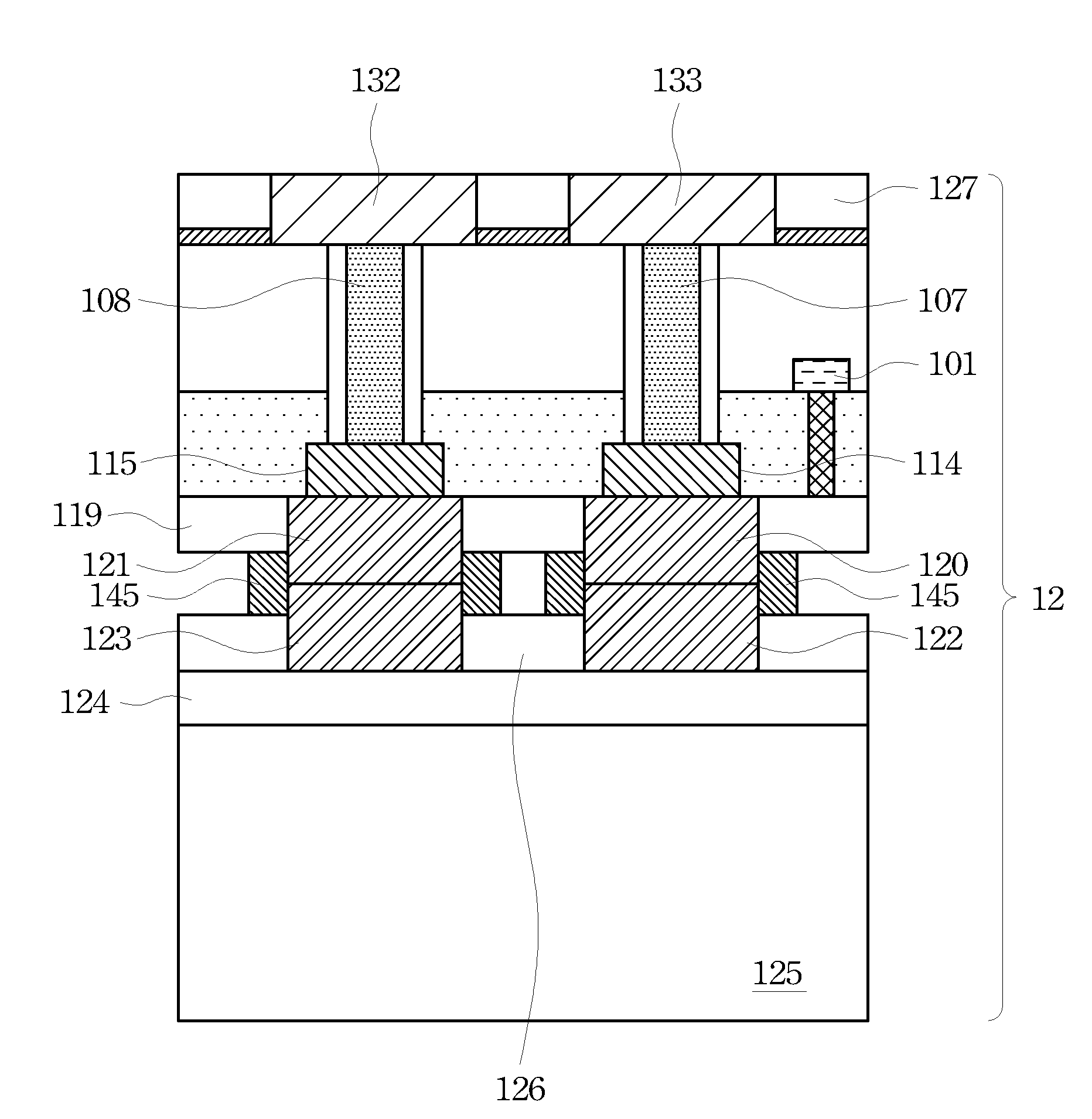
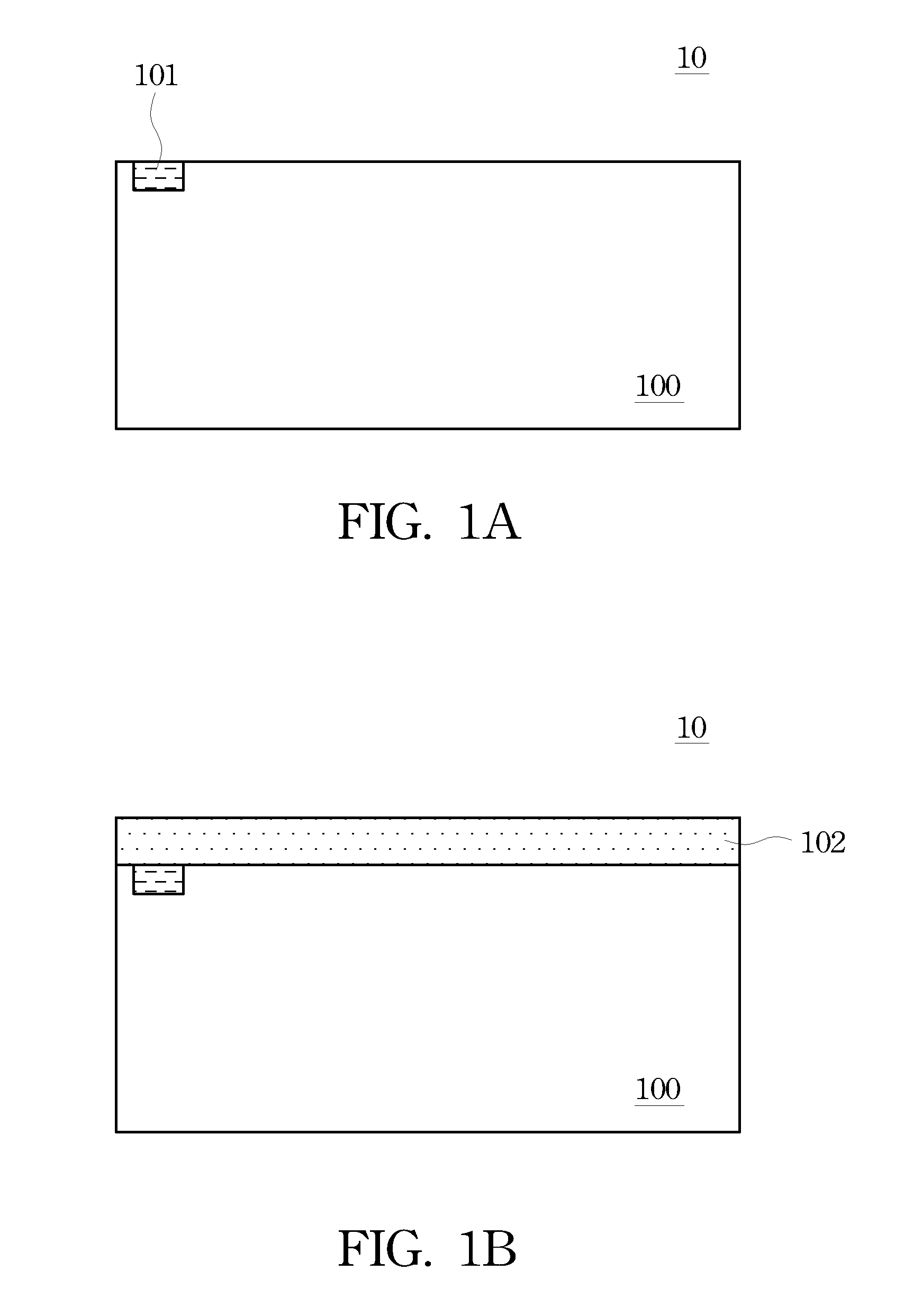
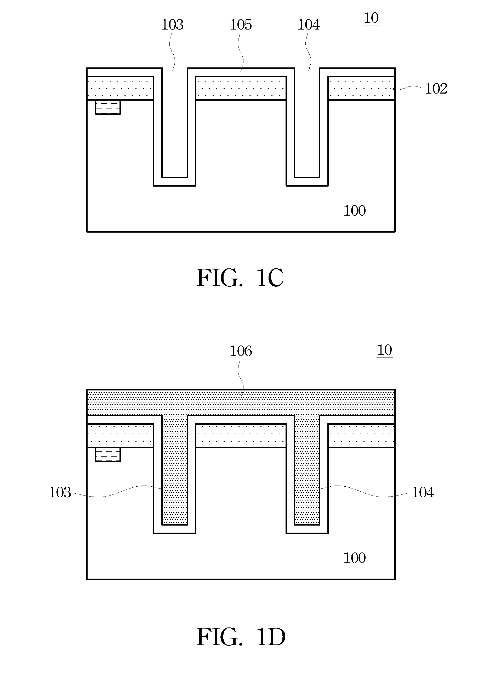
[0019]With reference now to FIG. 1A, there is shown a portion of a cross-sectional diagram of wafer 10. Wafer 10 comprises substrate 100, which is typically silicon (Si), but may also be made of gallium arsenide (GaAs), gallium arsenide-phosphide (GaAsP), indium phosphide (InP), gallium aluminum arsenic (GaAlAs), indium gallium phosphide (InGaP), and the like, and illustrates device 101 processed from substrate 100. Device 101 may comprises one or more known active and passive devices formed on substrate 100, such as transistors, diodes, resistors, capacitors, and inductors. ...


PUM


Abstract

The formation of bonding pad protective layer over exposed bonding pad materials between stacked integrated circuit (IC) dies or wafers is described in preferred embodiments in which the bonding pad protective layer is formed in the integrated process of forming wafer bonding pads. The bonding pad protective layer prevents the exposed bonding pad materials from oxidation and corrosion in open-air or other harsh environments. By providing a bonding pad protective layer on exposed bonding pad materials, significant product reliability improvement is expected on ICs having a three-dimensional “stacked-die” configuration.

Description

CROSS-REFERENCE TO RELATED APPLICATIONS[0001]This application relates to the following co-pending and commonly assigned patent application Ser. No. 11 / 769,559 filed on Jun. 27, 2007, entitled “Forming of Through Via before Contact Processing,” which application is hereby incorporated herein by reference.TECHNICAL FIELD[0002]The present invention relates generally to integrated circuit fabrication, and more particularly to forming protective layers for wafer and / or die bonding pads.BACKGROUND[0003]In modern integrated circuits, the speed at which an integrated circuit operates is generally limited, among other things, by the distance between the farthest separated components that communicate with each other on the chip. Laying out circuits as three-dimensional structures has been shown to significantly reduce the communication path length between on-chip components, provided the vertical distances between layers are smaller than the chip width of the individual layers. Thus, by stack...

Claims


Application Information

Patent Timeline
Patent Type & Authority Applications(United States)
IPC IPC(8): H01L23/488H01L21/60
CPCH01L21/76898H01L2224/8192H01L24/06H01L24/11H01L24/13H01L24/16H01L24/81H01L25/0657H01L25/50H01L2224/0401H01L2224/05624H01L2224/05639H01L2224/05647H01L2224/05684H01L2224/06181H01L2224/13025H01L2224/13099H01L2224/13147H01L2224/81054H01L2224/81203H01L2224/81801H01L2224/81894H01L2225/06513H01L2225/06541H01L2924/01013H01L2924/01014H01L2924/01027H01L2924/01029H01L2924/01033H01L2924/01049H01L2924/0105H01L2924/01074H01L2924/01079H01L2924/01082H01L2924/10329H01L23/3171H01L2924/01047H01L2924/01006H01L2924/01039H01L2924/14H01L2924/00
Inventor YU, CHEN-HUACHIOU, WEN-CHIHWU, WENG-JIN
Owner TAIWAN SEMICON MFG CO LTD
Why Eureka
Try Eureka