Pixel and organic light emitting display using the same

a technology pixels, applied in the field of pixels and organic light emitting displays, can solve the problems of degrading of light emitting diodes (oleds), difficult to display images with desired luminance, and difficult to achieve desired luminan

Active Publication Date: 2009-09-10
SAMSUNG DISPLAY CO LTD
View PDF18 Cites 84 Cited by
  • Summary
  • Abstract
  • Description
  • Claims
  • Application Information

AI Technical Summary

Benefits of technology

[0016]An embodiment of the present invention provides a pixel including an organic light emitting diode; a second transistor for controlling an electric current capacity flowing from a first power source to a second power source via the organic light emitting diode; a first capacitor coupled between a gate electrode of the second transistor and a power line or a control line; a first transistor coupled to a scan line and a data line and for turning on, when a scan signal is supplied to a scan line, to supply a data signal, supplied by the data line, to the gate electrode of the second transistor; and a compensation unit for controlling a voltage of the gate electrode of the second transistor to correspond to a degradation of the organic light emitting diode. The compensation unit includes first and second feedback capacitors coupled in series between an anode electrode of the organic light emitting diode and the gate electrode of the second transistor and a third transistor coupled between a common node of the first and second feedback capacitors and a reset power source and for turning on when a control signal is supplied to the control line.
[0017]The pixel according to one embodiment of the present invention further includes a fourth transistor coupled between the second transistor and the organic light emitting diode and for turning off when a light emitting control signal is supplied to a light emitting control line. Also, the pixel according to one embodiment of the present invention further includes a second capacitor coupled between the gate electrode of the second transistor and the first power source. Furthermore, the reset power source may be set to have substantially identical voltage as that of the first power source.
[0018]Another embodiment of the present invention provides an organic light emitting display including a scan driver for sequentially supplying a scan signal to scan lines and sequentially supplying a control signal to signal control lines; a data driver for supplying a data signal to data lines to synchronize with the scan signal; and pixels at crossing region of the scan lines and the data lines. Each of the pixels extended in an ith (i is an integer) horizontal line of the organic light emitting display includes an organic light emitting diode; a second transistor for controlling an electric current capacity flowing from a first power source to a second power source via the organic light emitting diode; a first capacitor coupled between a gate ele

Problems solved by technology

However, the above-mentioned organic light emitting display has a problem in that it is difficult to display an image with desired luminance due to the changes in efficiency caused by the degradation (or deterioration) of the organic light emitting diode (OLED).
That is, the organic light emitting di

Method used


Image

  • Pixel and organic light emitting display using the same
  • Pixel and organic light emitting display using the same
  • Pixel and organic light emitting display using the same

Examples


Embodiment Construction

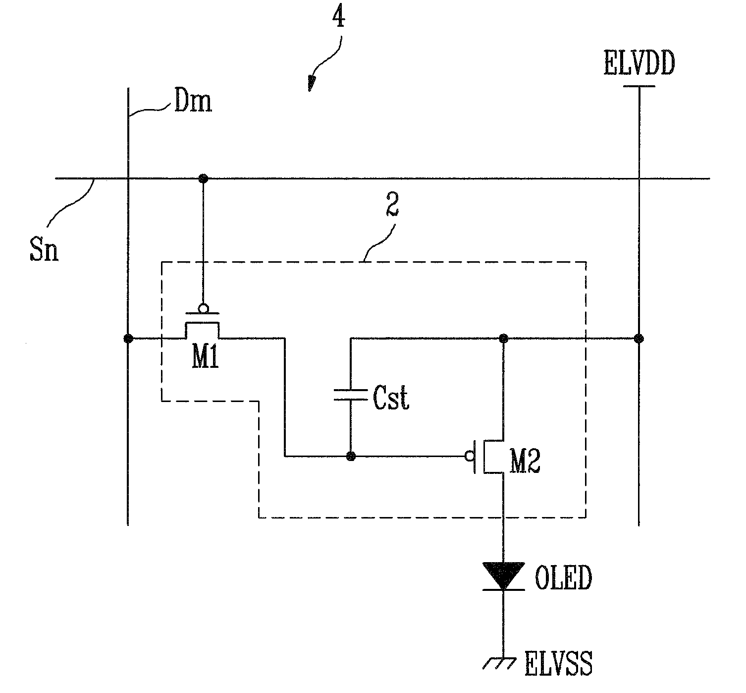
[0029]Hereinafter, certain exemplary embodiments according to the present invention will be described with reference to the accompanying drawings. Here, when a first element is described as being coupled to a second element, the first element may be not only directly coupled to the second element but may also be indirectly coupled to the second element via a third element. Further, some of the elements that are not essential to the complete understanding of the invention are omitted for clarity. Also, like reference numerals refer to like elements throughout.

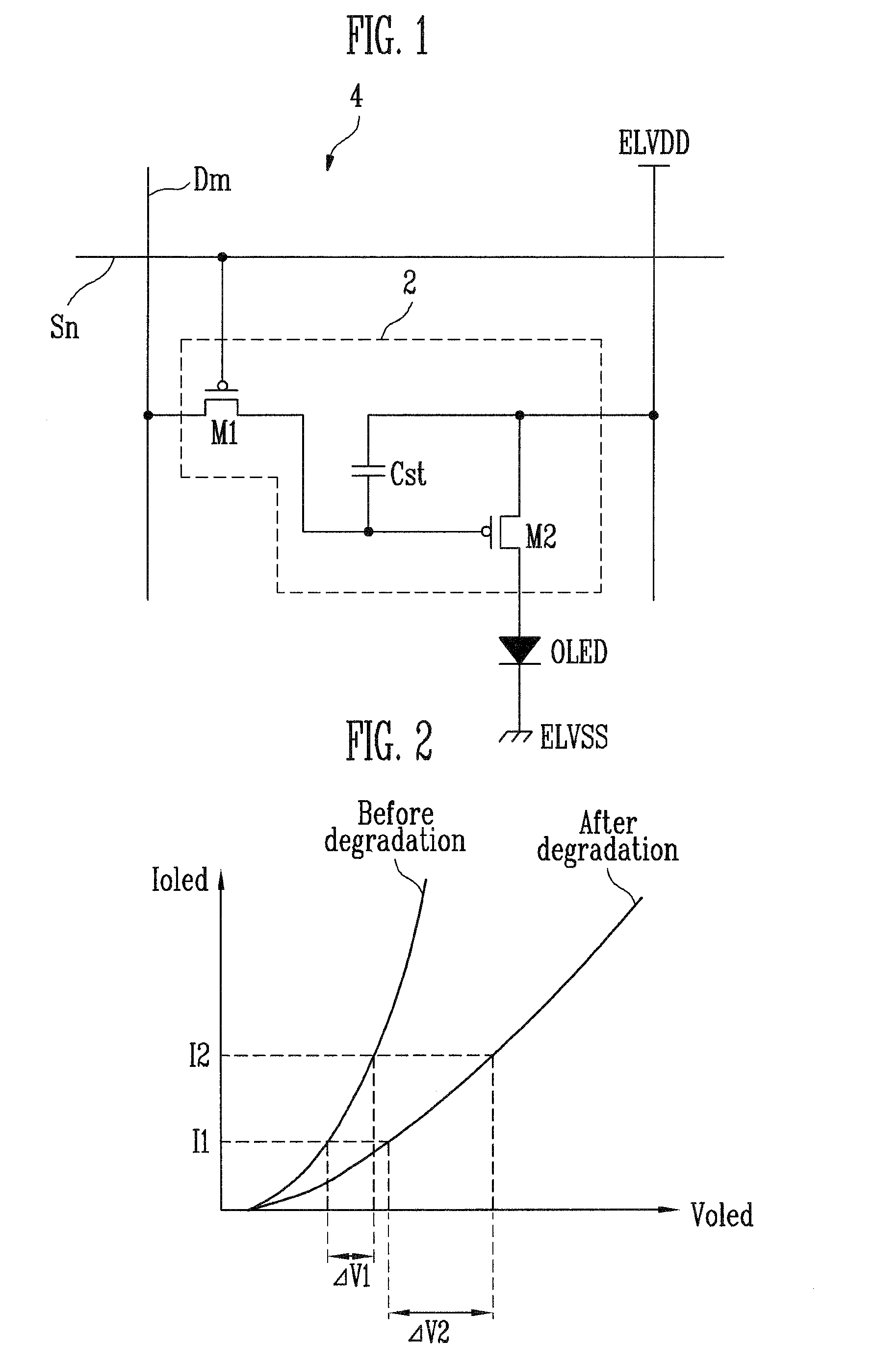
[0030]FIG. 2 is a graph illustrating the degradation characteristics of an organic light emitting diode. In FIG. 2, “Ioled” represents an electric current that flows in an organic light emitting diode, and “Voled” represents a voltage applied to the organic light emitting diode.

[0031]Referring to FIG. 2, a higher voltage is applied to an organic light emitting diode that is more degraded (after degradation) to correspond to the ...


PUM


Abstract

A pixel capable for compensating for the degradation of an organic light emitting diode. The pixel includes an organic light emitting diode; a pixel circuit including a driving transistor for controlling an electric current capacity flowing from a first power source to a second power source via the organic light emitting diode; and a compensation unit for controlling a voltage of a gate electrode of the driving transistor to correspond to a degradation of the organic light emitting diode. The compensation unit includes first and second feedback capacitors coupled in series between an anode electrode of the organic light emitting diode and the gate electrode of the driving transistor and a switching transistor coupled between a common node of the first and second feedback capacitors and a reset power source and for turning on when a control signal is supplied to a control line coupled to the switching electrode.

Description

CROSS-REFERENCE TO RELATED APPLICATIONS[0001]This application claims priority to and the benefit of Korean Patent Application No. 10-2008-0021974, filed on Mar. 10, 2008, in the Korean Intellectual Property Office, the entire content of which is incorporated herein by reference.BACKGROUND OF THE INVENTION[0002]1. Field of the Invention[0003]The present invention relates to a pixel and an organic light emitting display using the same, and more particularly to a pixel capable of compensating for the degradation of an organic light emitting diode, and an organic light emitting display using the same.[0004]2. Description of Related Art[0005]In recent years, there have been many attempts to develop various flat panel displays having a lighter weight and a smaller volume than that that of a cathode ray tube display. The flat panel displays include a liquid crystal display (LCD), a field emission display (FED), a plasma display panel (PDP), an organic light emitting display (OLED), etc.[00...

Claims


Application Information

Patent Timeline
IPC IPC(8): G09G3/30
CPCG09G3/3233G09G2320/045G09G2300/0819G09G2300/0814G09G3/20G09G3/30G09G3/32H05B33/12
Inventor CHOI, SANG-MOO
Owner SAMSUNG DISPLAY CO LTD
Why Eureka
Try Eureka